Metal film forming method of power MOS device
A MOS device and metal film forming technology, which is applied in semiconductor/solid-state device manufacturing, electrical components, circuits, etc., can solve problems such as weak bonding degree, improve electrical performance and service life, and improve bonding performance.
- Summary
- Abstract
- Description
- Claims
- Application Information
AI Technical Summary
Problems solved by technology
Method used
Image

Examples
Embodiment Construction
[0015] The present invention will be described in further detail below in conjunction with the accompanying drawings and embodiments.
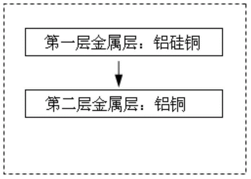
[0016] Such as image 3 Shown, a kind of metal film forming method of the present invention improves power MOS (power MOS) bonding performance, mainly comprises the following steps:
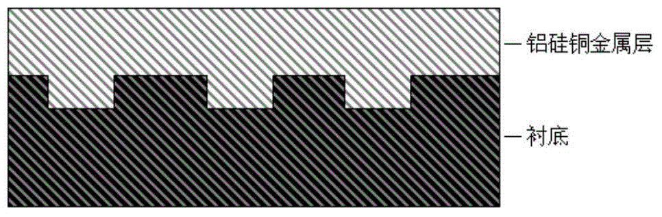
[0017] (1) The formation of the first metal layer, aluminum-silicon-copper; the film-forming substrate is a silicon substrate, and the film-forming substances on the surface include but are not limited to oxide film, polysilicon, metal titanium, titanium nitride and other substances; this step mainly adopts physical Sputtering film forming process, the film forming thickness is 10-40000 Angstroms, the sputtering temperature is 10-500°C, and the pressure is 1-100mtorr.
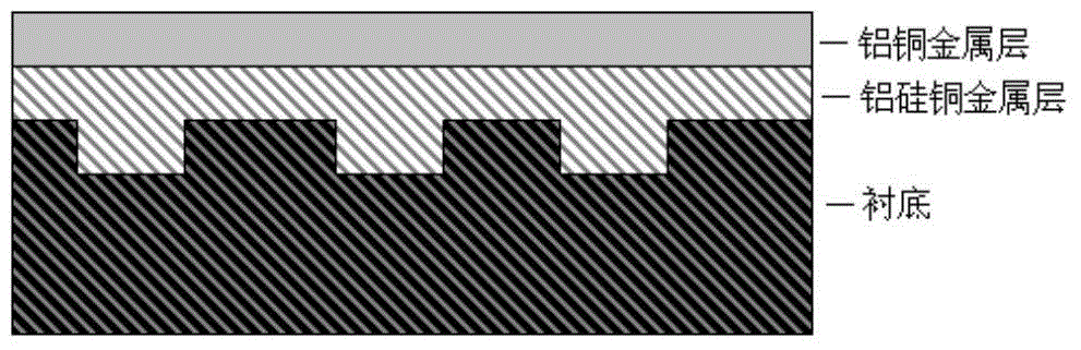
[0018] (2) The formation of the second metal layer of aluminum copper; this step mainly adopts the physical sputtering film forming process, the film thickness is 10-40000 angstroms, the sputteri...
PUM
| Property | Measurement | Unit |
|---|---|---|
| thickness | aaaaa | aaaaa |
Abstract
Description
Claims
Application Information