Resin composition, cured resin, sheet-like cured resin, laminated body, prepreg, electronic parts and multilayer boards

a technology of cured resin and cured resin, which is applied in the direction of synthetic resin layered products, solid-state devices, inductance, etc., can solve the problems of insufficient flexural strength or flexural modulus of the above-mentioned composite dielectric layer, and the material exhibits no superior strength in terms of strength, so as to prevent damage to multi-layer boards or electronic parts, the effect of satisfactorily maintaining electrical properties

Inactive Publication Date: 2005-01-06
TDK CORPARATION
View PDF2 Cites 135 Cited by
  • Summary
  • Abstract
  • Description
  • Claims
  • Application Information

AI Technical Summary

Benefits of technology

The second dielectric layer may further comprise a ceramic powder with a larger dielectric constant than the resin. This will allow the electrical properties to be satisfactorily maintained even when a resin with a low dielectric constant is used.
The aforementioned multilayer boards and electronic parts have two outermost layers, preferably with at least one of the two outermost layers being composed of the aforementioned first dielectric layer and at least one second dielectric layer being situated between the two outermost layers. This can adequately prevent damage of the multilayer boards or electronic parts, even when excessive loads are applied to the multilayer boards or electronic parts.
The peel strength of the first dielectric layer in such multilayer boards and electronic parts is preferably at least 1.5 times the peel strength of the second dielectric layer. This can satisfactorily maintain the electrical properties while even more adequately preventing damage of the multilayer boards or electronic parts, even when excessive loads are applied after completion of the products.
The invention also relates to multilayer boards and electronic parts constructed by laminating two resin-containing first dielectric layers, at least one resin-containing second dielectric layer situated between the two first dielectric layers, and at least one conductor layer, wherein at least one of the two first dielectric layers constitutes the outermost layer, the dielectric loss tangent tan δ of the second dielectric layers is no greater than 0.01 and the peel strengths of the first dielectric layers are at least 1.5 times the peel strengths of the second dielectric layers. For such multilayer boards and electronic parts, the peel strengths of the first dielectric layers are at least 1.5 times the peel strengths of the second dielectric layers and the dielectric loss tangents tan δ of the second dielectric layers are no greater than 0.01. That is, multilayer boards and electronic parts according to the invention comprise dielectric layers with excellent mechanical strength and dielectric layers with excellent electrical properties. It is therefore possible to satisfactorily maintain electrical properties while adequately preventing damage of the multilayer boards or electronic parts, even when excessive loads are applied after completion of the products.
The peel strengths of the first dielectric layers in such multilayer boards and electronic parts are preferably at least 8 N / cm. This will further increase the anchoring strength and peel strength of mounted passive elements and active elements, as well as the electrode strengths of the multilayer boards and electronic parts, as compared to when the peel strengths of the first dielectric layers are less than 8 N / cm.
The invention also relates to electronic parts which are provided with the aforementioned multilayer boards and electrical elements formed on the multilayer boards. In this case as well, since the multilayer boards comprise dielectric layers with excellent mechanical strength and dielectric layers with excellent electrical properties, it is possible to satisfactorily maintain electrical properties while adequately preventing damage of the multilayer boards or electronic parts, even when excessive loads are applied to the electronic parts after completion of the products.

Problems solved by technology

In addition, despite the satisfactory electrical properties, such as the dielectric constant and dielectric loss tangent (tan δ), of the composite dielectric layer in electronic parts employing the composite dielectric layer described in the aforementioned prior art publication, such materials exhibit no superiority in terms of strength.
Furthermore, the above-mentioned composite dielectric layer does not exhibit sufficient flexural strength or flexural modulus, and can therefore also be improved from the viewpoint of its adhesion with copper foils (peel strength, etc.).

Method used


Image

  • Resin composition, cured resin, sheet-like cured resin, laminated body, prepreg, electronic parts and multilayer boards
  • Resin composition, cured resin, sheet-like cured resin, laminated body, prepreg, electronic parts and multilayer boards
  • Resin composition, cured resin, sheet-like cured resin, laminated body, prepreg, electronic parts and multilayer boards

Examples


tenth embodiment

(Tenth Embodiment)

FIGS. 23 to 26 show a laminated filter as a tenth embodiment of an electronic part of the invention. FIG. 23 is a perspective view, FIG. 24 is an exploded perspective view,FIG. 25 is an equivalent circuit diagram and FIG. 26 is a transfer characteristic graph.

The laminated filter of this embodiment is constructed to have a four-pole type transfer characteristic. As shown in FIGS. 23 to 25, this laminated filter 60 differs from the laminated filter of the ninth embodiment which has two strip lines 68 formed on the component layer 60c, in that four strip lines 68 are formed on the component layer 60c.

In the laminated filter of this embodiment, the strip lines 68 are the strip lines 74c,74d,74e,74f having lengths of λg / 4 or less as shown in the equivalent circuit diagram of FIG. 25, and the strip lines 74c,74d, the strip lines 74d,74e and the strip lines 74e,74f are each linked by a coupling capacitance Cm and coupling coefficient M. Because the laminated filter ...

eleventh embodiment

(Eleventh Embodiment)

FIGS. 27 to 32 show a block filter as an eleventh embodiment of an electronic part of the invention. FIG. 27 is a perspective view, FIG. 28 is front cross-section view, FIG. 29 is a side cross-sectional view, FIG. 30 is a flat cross-sectional view, FIG. 31 is an equivalent circuit diagram and FIG. 32 is a side view showing the structure of the molding die.

The block filter of this embodiment is constructed to have a two-pole type transfer characteristic. As shown in FIGS. 27 to 32, the block filter 80 comprises a configuration block 80a, a pair of coaxial conductors 81 formed in the configuration block 80a and condenser coaxial conductors 82 connected to the coaxial conductors 81. The coaxial conductors 81 and condenser coaxial conductors 82 consist of conductors formed in a hollow fashion through the configuration block 80a. A surface GND conductor 87 is formed around the configuration block 80a so as to cover it. Condenser conductors 83 are formed at positio...

twelfth embodiment

(Twelfth Embodiment)

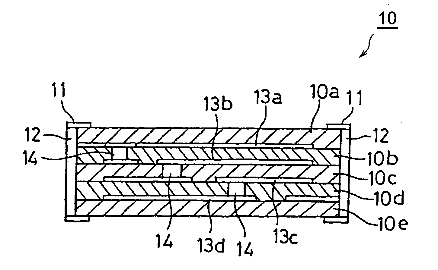
FIGS. 33 to 37 show a coupler as a twelfth embodiment of an electronic part of the invention. FIG. 33 is a perspective view, FIG. 34 is a cross-sectional view, FIG. 35 is an exploded perspective view showing each of the component layers, FIG. 36 is an internal connection diagram, and FIG. 37 is an equivalent circuit diagram.

In FIGS. 33 to 37, the coupler 110 comprises a laminated body obtained by laminating component layers 110a-110c, internal GND conductors 115 formed on the upper and lower surfaces of component layer 10b of the laminated body, and two coil patterns formed between the internal GND conductors 115, constituting a transformer. Each of the coil patterns is composed of a plurality of internal conductors 113 and a via hole 114 connecting the internal conductors 113, and each is in a spiral configuration. The ends of the formed coil patterns and the internal GND conductors 115 are connected to terminal electrodes 112 formed on the sides of the lamin...


PUM

PropertyMeasurementUnit
dielectric constantaaaaaaaaaa
thicknessaaaaaaaaaa

Abstract

The invention provides electronic parts which comprise a composite dielectric layer composed of an organic insulating material and a dielectric ceramic powder having a larger relative dielectric constant than the organic insulating material, and which also comprise conductive element sections forming inductor elements, etc., wherein the organic insulating material comprises a cured resin obtained by curing reaction of an epoxy resin with an active ester compound obtained by reaction between a compound with two or more carboxyl groups and a compound with a phenolic hydroxyl group. The dielectric ceramic powders of the described electronic parts have larger relative dielectric constants than the organic insulating materials, and the organic insulating materials have low dielectric loss tangents. It is possible to adequately reduce time-dependent dielectric constant changes in the high-frequency range of 100 MHz and above even with prolonged use at high temperatures of 100° C. and higher, while it is also possible to satisfactorily prevent deformation and other damage to the electronic parts during their handling.

Description

BACKGROUND OF THE INVENTION 1. Field of the Invention The present invention relates to a resin composition, a cured resin, a sheet-like cured resin, a laminated body, a prepreg, electronic parts and multilayer boards, and more specifically, it relates to a resin composition, a cured resin, a sheet-like cured resin, a laminated body, a prepreg, electronic parts and multilayer boards which are useful in the high-frequency range of 100 MHz and above. 2. Related Background Art The rapid increase in communication of information in recent years has led to a strong demand for smaller and more lightweight communicating devices and a concomitant demand for smaller and more lightweight electronic parts. At the same time, electromagnetic waves in the high-frequency range of the gigahertz band have come to be utilized for portable mobile communications and satellite communications. In order to handle such high-frequency electromagnetic waves, it is essential for electronic parts to have lo...

Claims


Application Information

Patent Timeline
Patent Type & Authority Applications(United States)
IPC IPC(8): B32B15/08C08G59/42C08J5/24C08L63/00C08L67/03H01F17/00H01F27/32H01L23/498H01L25/16H05K1/00H05K1/03H05K1/16H05K3/46
CPCB32B15/08Y10T428/2971C08J5/10C08J5/18C08J5/24C08J2363/00C08L63/00C08L67/03H01F17/0006H01F27/323H01F27/327H01F2017/048H01L23/49894H01L25/16H01L2224/32225H01L2224/48091H01L2224/48227H01L2224/73265H01L2924/01012H01L2924/0102H01L2924/01025H01L2924/01046H01L2924/01078H01L2924/01079H01L2924/19041H01L2924/19105H01L2924/30107H01L2924/3011H01L2924/3025H05K1/0373H05K1/162H05K3/4626H05K3/4676H05K3/4688H05K2201/0209H05K2201/09672C08G59/4223H01L2924/12041H01L2924/01068H01L2924/01019H01L24/48C08L2666/18H01L2924/00014H01L2924/00H01L2924/12042H01L2924/181Y10T428/31529Y10T428/31522Y10T428/31515Y10T428/31511C08J5/244C08J5/249H01L2924/00012H01L2224/45099H01L2224/45015H01L2924/207C08K7/18B32B15/092C08J2367/03B32B2305/08B32B2305/076B32B27/08B32B2307/204B32B2307/206B32B2307/202B32B9/005
Inventor TAKAYA, MINORUENDO, TOSHIKAZUKAWABATA, KENICHI
Owner TDK CORPARATION
Why Eureka
Try Eureka