Semiconductor structure

a technology of semiconductors and structures, applied in semiconductor devices, instruments, electrical equipment, etc., can solve the problems of increasing manufacturing costs and affecting and achieve the effect of maintaining the electrical properties of the structure and reducing the area of ground lines

Active Publication Date: 2016-06-14
MACRONIX INT CO LTD
View PDF7 Cites 1 Cited by
  • Summary
  • Abstract
  • Description
  • Claims
  • Application Information

AI Technical Summary

Benefits of technology

[0007]The disclosure is directed to a semiconductor structure with specific ground lines and bit lines arrangement, which is capable of reducing the area of ground line and maintain the electrical property of the structure.

Problems solved by technology

However, the bulk end and the source end may not connect directly in some circuit design.
Nevertheless, the huge metal ground lines in prior art not only take the effective area of circuit, but also influence the nearby bit line.
Therefore, bit lines being adjacent to the ground lines have to be designed as dummy line, which increases the manufacturing cost.

Method used


Image

  • Semiconductor structure
  • Semiconductor structure
  • Semiconductor structure

Examples


Embodiment Construction

[0014]In the following detailed description, for purposes of explanation, numerous specific details are set forth in order to provide a thorough understanding of the disclosed embodiments. It will be apparent, however, that one or more embodiments may be practiced without these specific details. In other instances, well-known structures and devices are schematically shown in order to simplify the drawing.

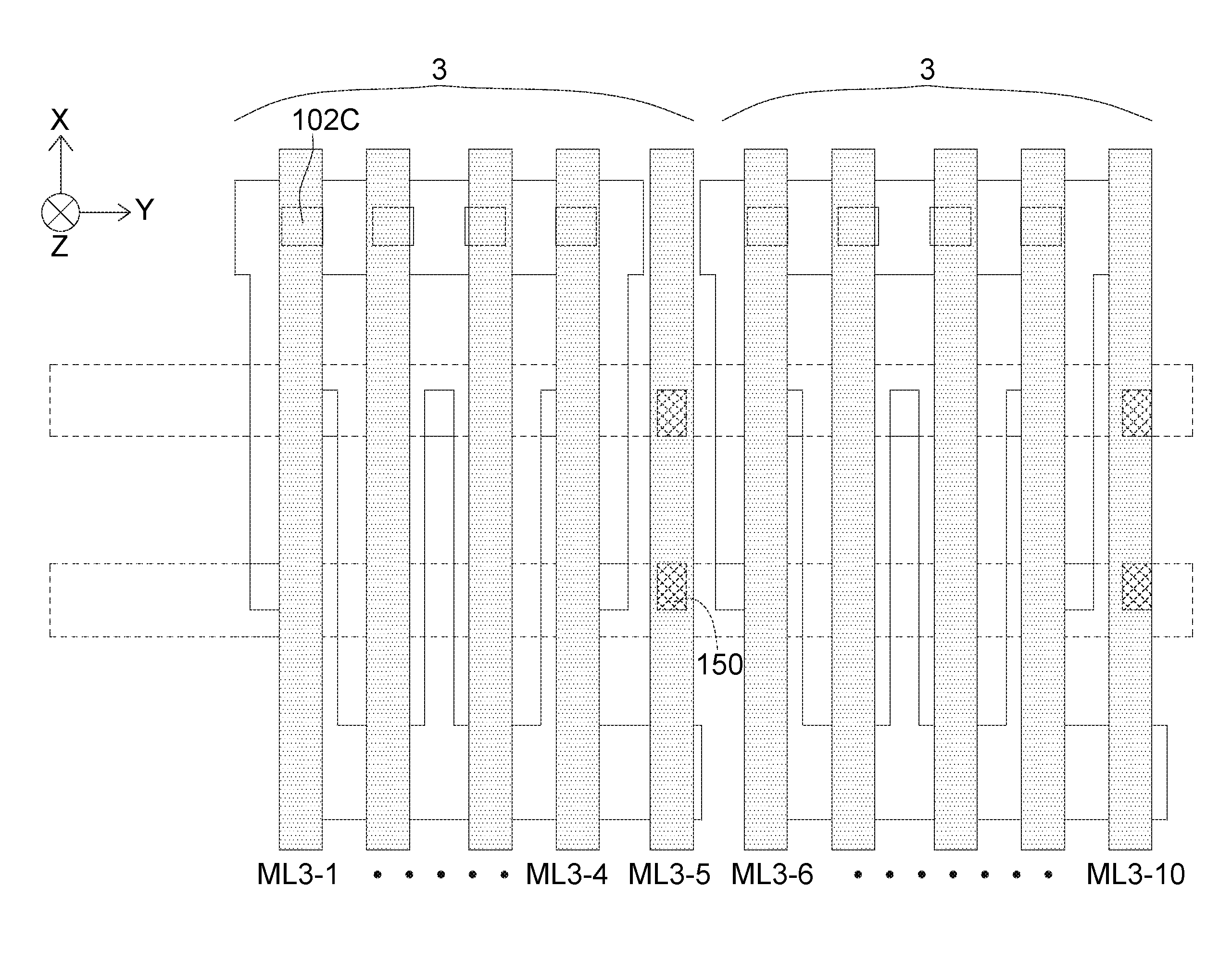
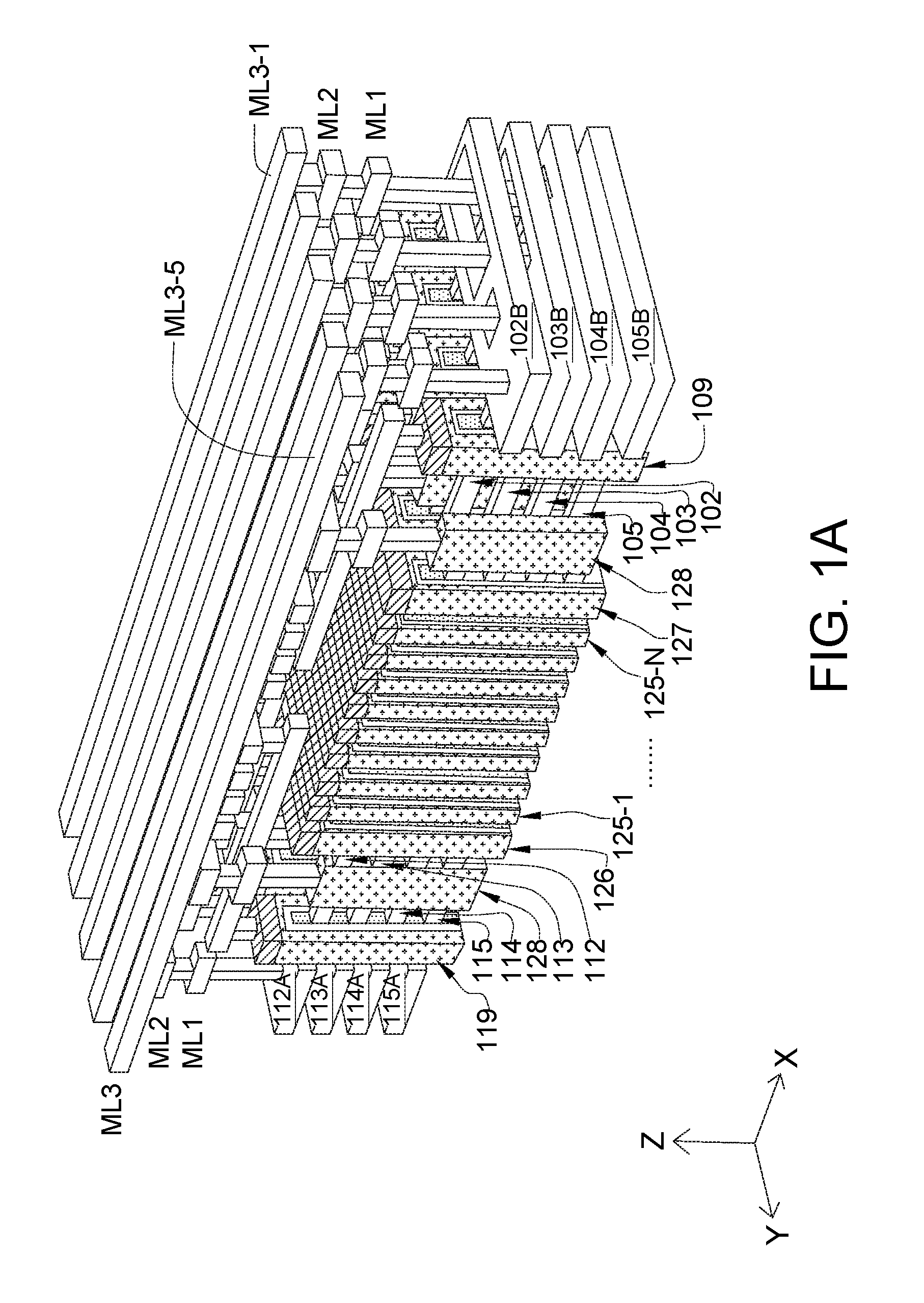
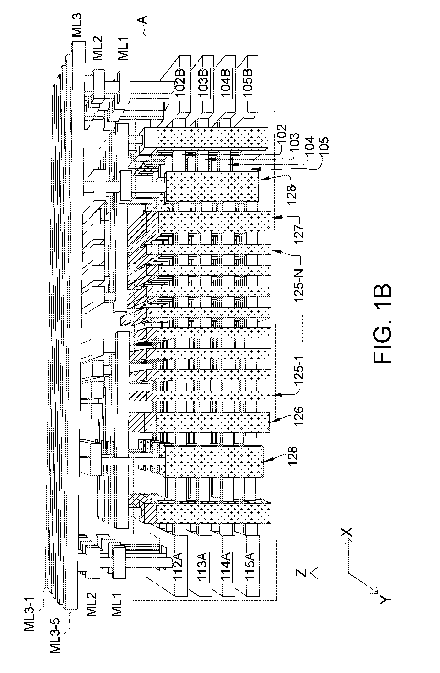
[0015]Referring to FIGS. 1A and 1B, FIG. 1A shows a schematic diagram of a semiconductor according to an embodiment; FIG. 1B is side illustrations of the semiconductor structure shown in FIG. 1A. Semiconductor structure 1 is a 3D NAND-flash memory device with finger vertical gate (Finger VG). The Finger VG structure is described in U.S. Pat. Nos. 8,383,512 and 8,503,213, which is commonly owned by the assignee of the present application and incorporated by reference herein. Insulating material in semiconductor structure 1 is removed from the drawing to expose additional structure. F...


PUM


Abstract

A semiconductor device comprises a plurality of stacking blocks and a plurality of conductive lines. Each stacking blocks comprises two opposite finger VG structures. Each finger VG structure includes a staircase structure and a plurality of bit line stacks. The staircase structure is perpendicular to the bit line stacks, and the bit line stacks of the two opposite finger VG structures are arranged alternately. The conductive lines is disposed over the stacking blocks at interval. The direction of the conductive lines is parallel to a direction of the bit line stacks. The conductive lines include a plurality of bit lines and a plurality of ground lines, and each stacking block includes at least one ground line.

Description

BACKGROUND[0001]1. Technical Field[0002]The disclosure relates in general to a semiconductor structure, and more particularly to a semiconductor structure designed for memory device with bit lines and ground lines.[0003]2. Description of the Related Art[0004]In typical MOSFET (metal-oxide-semiconductor field-effect transistor), the bulk end (body or substrate) and the source end have the same electric potential, and the voltage of source-body junction is zero.[0005]However, the bulk end and the source end may not connect directly in some circuit design. In this situation, the extra loading in circuit may generate bias at source end (VS), resulting in changes in threshold voltage (VT). This phenomenon is called body effect.[0006]When a plurality of transistors are connected in series (such as the bit lines in memory device), the body effect may significantly change the VT of transistor, influences the character of circuit. Thus, it is necessary to diminish the body effect. The tradit...

Claims


Application Information

Patent Timeline
Patent Type & Authority Patents(United States)
IPC IPC(8): H01L27/105H01L27/115G11C16/04
CPCH01L27/11565H01L27/11578H01L27/11556G11C16/0483H10B43/10H10B43/20H10B41/27
Inventor CHEN, SHIH-HUNG
Owner MACRONIX INT CO LTD
Why Eureka
Try Eureka