Al technical title is built by PatSnap Al team. It summarizes the technical point description of the patent document.
A technology of boosting circuit and resistor, applied in the field of circuits, can solve problems such as low boosting efficiency
Active Publication Date: 2015-06-03
GIGADEVICE SEMICON (BEIJING) INC
View PDF5 Cites 1 Cited by
Summary
Abstract
Description
Claims
Application Information
AI Technical Summary
This helps you quickly interpret patents by identifying the three key elements:
Problems solved by technology
Method used
Benefits of technology
Problems solved by technology
[0006] The invention provides a boosting circuit and a nonvolatile memory to solve the problem of low boosting efficiency of the boosting circuit using a charge pump at present
Method used
Image
Click on the blue label to locate the original text in one second.
Reading with bidirectional positioning of images and text.
Examples
Embodiment 1
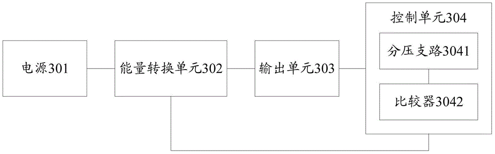
[0041] refer to image 3 , shows a structural block diagram of a boost circuit according to Embodiment 1 of the present invention.
[0042] In the embodiment of the present invention, the boost circuit may include: a power supply 301 , an energy conversion unit 302 , an output unit 303 and a control unit 304 . Wherein, the power supply 301, the energy conversion unit 302, the output unit 303 and the control unit 304 are connected in sequence, and the control unit 304 is connected to the energy conversion unit 302, and the output of the control unit 304 is connected to the energy conversion unit 302 .
[0043] Wherein, the control unit 304 includes a voltage dividing branch 3041 and a comparator 3042 connected thereto. The voltage division branch is used to divide the output voltage of the output unit to obtain a divided voltage, and input the divided voltage to the negative input terminal of the comparator, and the positive input terminal of the comparator to input preset r...
Embodiment 2
[0050] The boost circuit in the embodiment of the present invention may include: a power supply, an energy conversion unit, an output unit, and a control unit connected in sequence, and the control unit is connected to the energy conversion unit, and the output of the control unit is connected to the An energy conversion unit; wherein, the control unit includes a connected voltage dividing branch and a comparator.
[0051] Below, combine Figure 4 The boost circuit of the embodiment of the present invention is described in detail.
[0052] refer to Figure 4 , shows a circuit diagram of a boost circuit according to Embodiment 2 of the present invention.
[0053] (1 pair Figure 4 The individual components in are explained:
[0054] V IN :power supply;
[0055] L: inductance, in a specific implementation of the present invention, the inductance can be a bonded wire inductance, so that the area occupied by the boost circuit can be saved;
[0056] MN: MOS transistor (MOS t...
PUM
Abstract
The invention provides a voltage boosting circuit and a nonvolatile memory, aiming to solve the problem of low boosting efficiency of a voltage boosting circuit using a charge pump used at present. The voltage boosting circuit comprises a power supply, an energy conversion unit, an output unit and a control unit which are sequentially connected with one another, wherein the control unit is connected to the energy conversion unit; the control unit comprises a voltage division branch and a comparator which are connected; the voltage division branch is used for dividing the output voltage of the output unit to obtain component voltage; the component voltage is input into a negative input end of the comparator; preset reference voltage is input into a positive input end of the comparator; the output of the control unit is connected to the energy conversion unit. The voltage boosting circuit is capable of boosting voltage supplied by a power supply to required voltage; compared with the voltage boosting circuit using the charge pump, the voltage boosting circuit has the advantages that the output voltage is just detected by the voltage division branch, the energy conversion unit is controlled by the control unit according to different conditions, and the voltage boosting circuit is few in charge transmission stages and high in voltage boosting efficiency.
Description
technical field [0001] The invention relates to the technical field of circuits, in particular to a boost circuit and a nonvolatile memory. Background technique [0002] Non-volatile memory refers to a memory that can still retain data after power failure, that is, the stored data will not be lost after power failure. Both Flash Memory (flash memory) and EEPROM (Electrically Erasable Programmable Read-Only Memory, Electrically Erasable Programmable Read-Only Memory) are non-volatile memories. Flash Memory is a variant of EEPROM. The difference between Flash Memory and EEPROM is that EEPROM can be deleted and rewritten at the byte level instead of erasing the entire chip, while Flash Memory requires block erasing. [0003] When performing operations such as reading, writing, and deleting data on non-volatile memories such as Flash Memory and EEPROM, a higher voltage is required to meet the requirements, but the voltage provided by the general power supply cannot meet the abo...
Claims
Application Information
Patent Timeline
Application Date:The date an application was filed.
Publication Date:The date a patent or application was officially published.
First Publication Date:The earliest publication date of a patent with the same application number.
Issue Date:Publication date of the patent grant document.
PCT Entry Date:The Entry date of PCT National Phase.
Estimated Expiry Date:The statutory expiry date of a patent right according to the Patent Law, and it is the longest term of protection that the patent right can achieve without the termination of the patent right due to other reasons(Term extension factor has been taken into account ).
Invalid Date:Actual expiry date is based on effective date or publication date of legal transaction data of invalid patent.