Three-dimensional packaging chip silicon through hole testing device

A technology of three-dimensional packaging and testing equipment, which is applied in semiconductor/solid-state device testing/measurement, electrical components, circuits, etc., can solve problems such as module failure and 3D chip failure, and achieve the effect of optimizing the manufacturing process

Inactive Publication Date: 2015-06-10
SINO IC TECH
View PDF3 Cites 3 Cited by
  • Summary
  • Abstract
  • Description
  • Claims
  • Application Information

AI Technical Summary

Problems solved by technology

[0004] Different methods have their own different characteristics. Due to the limitation of the manufacturing process level, some failed TSVs will appear after the completion of the fabrication. These failed TSVs will lead to the failure of the interconnected modules or even the failure of the entire 3D chip.

Method used


Image

  • Three-dimensional packaging chip silicon through hole testing device

Examples


Embodiment Construction

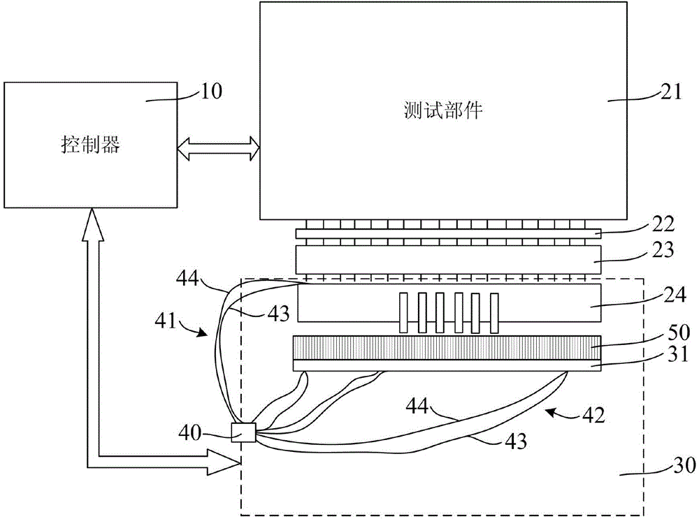
[0017] The test device for TSVs of three-dimensional packaged chips of the present invention will be described in more detail below in conjunction with schematic diagrams, wherein a preferred embodiment of the present invention is shown, and it should be understood that those skilled in the art can modify the present invention described here and still realize Advantageous effects of the present invention. Therefore, the following description should be understood as the broad knowledge of those skilled in the art, but not as a limitation of the present invention.

[0018] In the interest of clarity, not all features of an actual implementation are described. In the following description, well-known functions and constructions are not described in detail since they would obscure the invention with unnecessary detail. It should be appreciated that in the development of any actual embodiment, numerous implementation details must be worked out to achieve the developer's specific g...


PUM


Abstract

The invention provides a three-dimensional packaging chip silicon through hole testing device. A probe card and a chip carrying table are connected to a first testing signal line and a second testing signal line on the probe card and the chip carrying table respectively to form a testing loop, a testing signal of a testing part can be transmitted to the lower surface of wafer silicon through holes to be tested on the chip carrying table through the probe card, the first testing signal line and the second testing signal line, a probe of the probe card can gradually test the upper surfaces of silicon through holes of a wafer to be tested, accordingly the quality of the three-dimensional packaging chip silicon through holes can be accurately inspected, and the disqualification cause of the silicon through holes is further found according to an obtained result for manufacturing process optimization.

Description

technical field [0001] The invention relates to the field of semiconductor manufacturing and testing, in particular to a testing device for through-silicon vias in three-dimensional packaging chips. Background technique [0002] Three-dimensional packaged chips (3D chips) have gradually attracted people's attention and research due to their advantages of higher density, higher transmission rate and low power consumption, and Through Silicon Via (TSV) technology can make chips in three-dimensional The density of stacking in the direction is the highest, so that the interconnection lines between chips are the shortest and the external dimensions are the smallest, which can effectively realize the stacking of such 3D chips, and produce 3D chips with more complex structures, stronger performance, and more cost-effective. In the preparation process of three-dimensional packaging chips, there are currently four different TSV interconnection manufacturing technologies: wet etching ...

Claims


Application Information

Patent Timeline
IPC IPC(8): H01L21/66
CPCH01L22/10H01L22/14
Inventor 余琨祁建华张志勇叶守银刘远华罗斌
Owner SINO IC TECH
Why Eureka
Try Eureka