A high-concentration n-type doped thin germanium material on an insulating layer and its manufacturing method
An insulating layer, manufacturing method technology, applied in the field of materials, can solve the problems of rough material surface, immature technology, expensive equipment, etc., and achieve the effects of high crystal quality, increased activation rate, and reduced production costs
- Summary
- Abstract
- Description
- Claims
- Application Information
AI Technical Summary
Problems solved by technology
Method used
Image
Examples
Embodiment 1
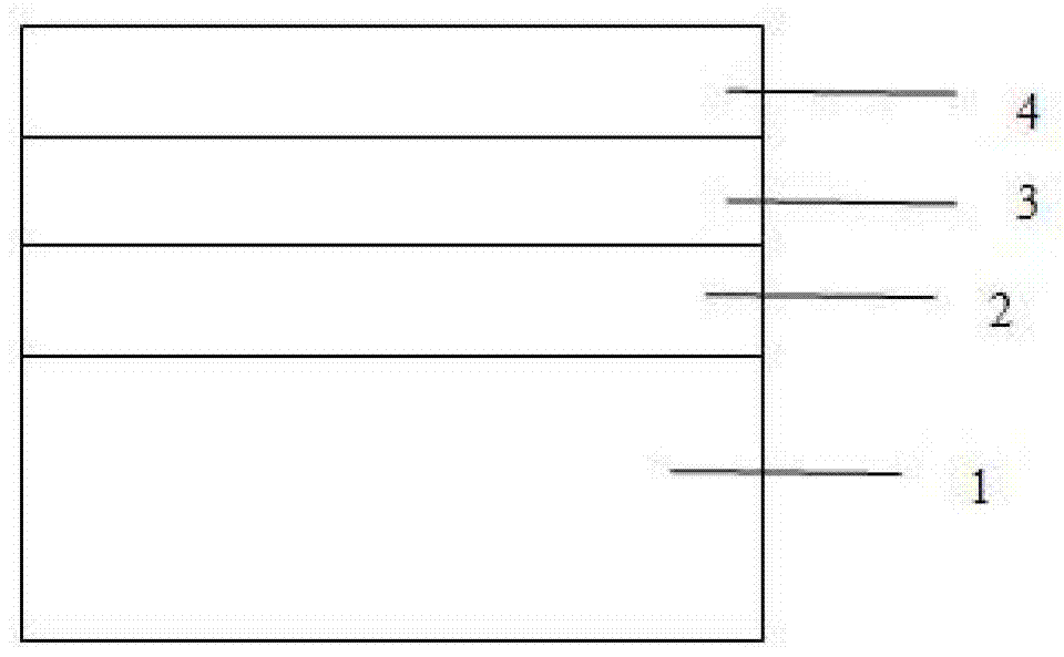
[0029] like figure 1 A high-concentration N-type doped thin germanium material on the insulating layer is shown, and the structure of the high-concentration N-type doped thin germanium material on the insulating layer is silicon substrate 1 from bottom to top, preventing N-type impurity atoms Buried SiO diffused into Si substrate 2 2. N-type doped germanium film 3 and SiO produced by oxidation 2 Layer 4, the buried SiO 2 2 has a thickness of 200nm, and the thickness of the N-type doped germanium film 3 is 30nm; the doping element in the N-type doped germanium film 3 is arsenic, and the concentration of the doping element is 10 17 cm ‐3 .
Embodiment 2
[0031] likefigure 1 A high-concentration N-type doped thin germanium material on the insulating layer is shown, and the structure of the high-concentration N-type doped thin germanium material on the insulating layer is silicon substrate 1 from bottom to top, preventing N-type impurity atoms Buried SiO diffused into Si substrate 2 2. N-type doped germanium film 3 and SiO produced by oxidation 2 Layer 4, the buried SiO 2 2 has a thickness of 400nm, the thickness of the N-type doped germanium film 3 is 20nm, the doping element in the N-type doped germanium film 3 is phosphorus, and the concentration of the doping element is 10 18 cm ‐3 .
Embodiment 3
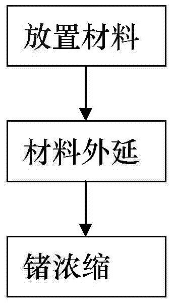
[0033] like figure 2 A method for manufacturing a high-concentration N-type doped thin germanium material on an insulating layer includes the following steps:
[0034] Step 1) placing materials: put in SOI substrate, the SOI substrate is silicon substrate, buried layer SiO2 from bottom to top 2 and top-layer silicon; the top-layer silicon is N-type doped silicon; the doping element of the N-type doped silicon is phosphorus atoms; the doping concentration of the phosphorus atoms is 4.0×10 19 cm -3 ;
[0035] The buried SiO 2 The thickness is 400nm, the thickness of the N-type doped silicon is 40nm, the N-type doping is obtained by ion implantation, the implanted ions are phosphorus ions, the implantation energy is 32Kev, and the implantation dose is 5x10 14 cm -2 , corresponding to a doping concentration of 4.0x10 19 cm -3 .
[0036] Step 2) material epitaxy: epitaxial germanium-silicon alloy thin film and Si cover layer successively on the top layer silicon of SOI sub...
PUM
| Property | Measurement | Unit |
|---|---|---|
| thickness | aaaaa | aaaaa |
| thickness | aaaaa | aaaaa |
| thickness | aaaaa | aaaaa |
Abstract
Description
Claims
Application Information

