P-type nitride semiconductor and method of manufacturing the same

a nitride semiconductor and nitride technology, applied in the field of p-type nitride semiconductor, can solve the problems of difficult to obtain a good crystal and difficult to provide a low resistivity nitride semiconductor, and achieve the effect of improving the activation ra

Inactive Publication Date: 2006-08-17
PANASONIC CORP
View PDF11 Cites 14 Cited by
  • Summary
  • Abstract
  • Description
  • Claims
  • Application Information

AI Technical Summary

Benefits of technology

[0010] By so doing, a low resistance p-type nitride semiconductor layer is formed on a substrate in an atmosphere containing specific amount of hydrogen that suppresses the p-type dopant from being inactivated, and the hole carrier concentration of the p-type nitride semiconductor layer decreases to a level at which the low resistivity property can be maintained. In this way, a p-type nitride semiconductor having a superior crystal quality is made available without needing any post annealing treatment.
[0018] By so doing, the inactivation in a p-type nitride semiconductor due to hydrogen can be suppressed, and the low resistivity property of relatively high hole carrier concentration in a p-type nitride semiconductor layer is well maintained.
[0020] By so doing, dissociation of nitrogen from the surface of the grown p-type nitride semiconductor can be suppressed, as a result, deterioration of the surface can be prevented.
[0024] This makes it possible for a p-type nitride semiconductor to maintain the low resistivity property within a certain range, where it can function as a practical p-type semiconductor.
[0028] In the conventional p-type nitride semiconductor manufactured through the processes accompanied by the post annealing treatment, hydrogen concentration at the vicinity of exposed upper surface is greater by more than 10 times that inside the p-type nitride semiconductor. However, in a p-type nitride semiconductor of the present invention, the hydrogen concentration at the vicinity of the upper surface of p-type nitride semiconductor remains at the same level, or within approximately 10 times, as that inside of the p-type nitride semiconductor. Therefore, in accordance with the present invention, a p-type nitride semiconductor having an improved activation rate with the p-type dopant is provided.

Problems solved by technology

As is well known, it is not easy to provide a low resistivity nitride semiconductor because, in the p-type nitride semiconductor doped with magnesium, Mg, or other acceptor, the activation rate the acceptor is significantly lower relative to doner.
The above describe conventional method for manufacturing a p-type nitride semiconductor eliminating the post annealing, however, has following problems.
What is more, if a p-type nitride semiconductor is grown in a low hydrogen concentration the surface migration turns out to be insufficient, and certain specific atoms are not disposed at respective optimum points on the surface, making it difficult to obtain a good crystal.

Method used


Image

  • P-type nitride semiconductor and method of manufacturing the same
  • P-type nitride semiconductor and method of manufacturing the same
  • P-type nitride semiconductor and method of manufacturing the same

Examples


embodiment 1

[0039] A first exemplary embodiment of the present invention is described with reference to the drawings.

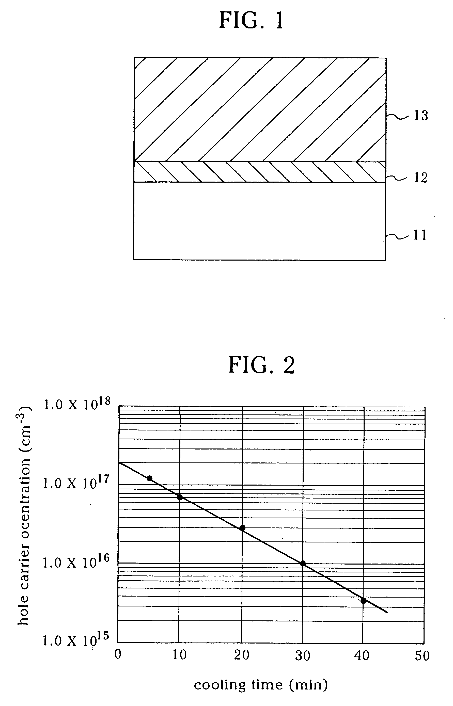
[0040]FIG. 1 is a cross sectional view showing the structure of a p-type nitride semiconductor in accordance with a first exemplary embodiment of the present invention. On a substrate 11 made of sapphire, a buffer layer 12 formed of gallium nitride (GaN) for easing the lattice mismatch between a certain semiconductor to be grown on the substrate 11 and the sapphire, and a p-type nitride semiconductor layer 13 formed of GaN are stacked in the order.

[0041] Method for manufacturing the above p-type nitride semiconductor layer is described in the following. In the first place, the substrate 11 having a mirror-finished main surface is placed in a reaction chamber (not shown) and held by a substrate holder, and then temperature of the substrate 11 is raised to approximately 1000° C., and hydrogen gas is introduced on the substrate 11 while it is heated for approximately 10 min. Stain...

first modification of embodiment 1

[0049] Method for manufacturing p-type nitride semiconductor layer in accordance with a first modification example of embodiment 1 is described below.

[0050] First buffer layer 12 and p-type nitride semiconductor layer 13 having the hole carrier concentration of approximately 2×1017 cm−3 are formed in the order on the substrate 11, as shown in FIG. 1, through the same method as in embodiment 1.

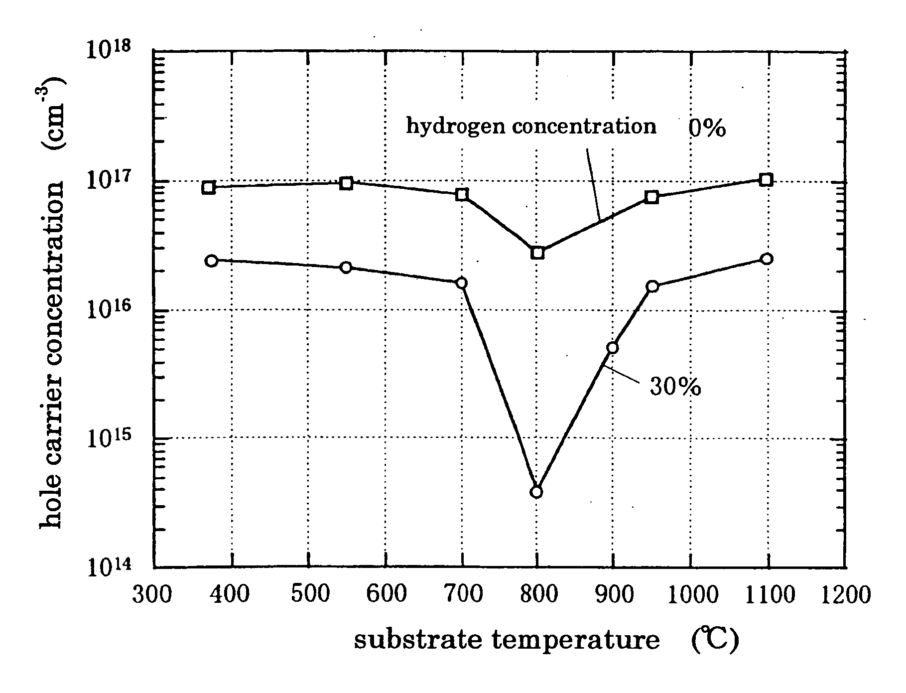
[0051] Dependence, during the cooling process in the first modification example, of the hole carrier concentration on concentration of hydrogen gas contained in the ambient gas is described below. The hole carrier concentration was measured with those which have undergone four different atmospheres having different hydrogen gas concentration, 0%, 30%, 50% and 70%. Concentration of ammonia, NH3, gas in each of the atmosphere was approximately 20%, and remainder of nitrogen gas. The substrate was cooled from approximately 1050° C., or the growth temperature, to approximately 600° C. in approxim...

second modification of embodiment 1

[0058] Method for manufacturing p-type nitride semiconductor layer in accordance with a second modification example of embodiment 1 is described below.

[0059] First buffer layer 12 and p-type nitride semiconductor layer 13 having the hole carrier concentration of approximately 2×1017 cm−3 are formed in the order on the substrate 11, as shown in FIG. 1, through the same method as in embodiment 1.

[0060] Dependence, during the cooling process in the second modification example, of the hole carrier concentration on concentration of ammonia, NH3, gas contained in the atmosphere is described. Concentration of hydrogen gas in the atmosphere was approximately 15%, and remainder of nitrogen gas. The substrate was cooled from approximately 1050° C., or the growth temperature, to approximately 600° C. in approximately 5 min.

[0061] As a result of the measurement, it has been confirmed that there is hardly any difference in the rate of decrease during the cooling process in the hole carrier co...


PUM

PropertyMeasurementUnit
temperatureaaaaaaaaaa
hole carrier concentrationaaaaaaaaaa

Abstract

A method for manufacturing p-type nitride semiconductor comprising a semiconductor layer forming process where a low resistivity p-type nitride semiconductor layer is formed on a substrate by introducing the sources of p-type dopant, nitrogen and Group III sources on a substrate held at a temperature of 600° C. or higher and a cooling process for cooling the substrate which is bearing the p-type nitride semiconductor layer. The manufacturing method features in that the hole carrier concentration of the p-type nitride semiconductor layer decreases during the cooling process. A superior quality p-type nitride semiconductor is made available, without needing any annealing treatment after growth, by properly specifying the concentration of atmosphere gas and the cooling time.

Description

FIELD OF THE INVENTION [0001] The present invention relates to a p-type nitride semiconductor, among the gallium nitride-based(Group III-V) semiconductor for use in light emitting devices emitting blue light or other light of short wavelength; more specifically, a p-type nitride semiconductor that does not require annealing treatment after growth. A method for manufacturing the semiconductor is also included in the present invention. BACKGROUND OF THE INVENTION [0002] Gallium nitride-based(Group III-V) semiconductor, which has a relatively large bandgap, is one of the prospective materials suitable for the short wavelength light emitting devices used in optical information processing units handling the increasing amount of information contents. In such light emitting devices as a diode device or a laser device, a PN junction is the essential structure, where the carriers are recombined at the vicinity of the junction and the light is emitted. As is well known, it is not easy to prov...

Claims


Application Information

Patent Timeline
Patent Type & Authority Applications(United States)
IPC IPC(8): H01L21/00H01L21/20
CPCH01L21/0242H01L21/02458H01L21/0254H01L21/02579H01L21/0262H01L33/007
Inventor KAMEI, HIDENORISHINAGAWA, SHUICHITAKEISHI, HIDEMI
Owner PANASONIC CORP
Why Eureka
Try Eureka