Voltage buffer circuit and circuit including voltage buffer circuit to be used for driving loads to be switched along with time sequence

A voltage buffering and load-driving technology, applied in logic circuits, electrical components, pulse technology, etc., can solve problems such as waste of static current and power consumption, and achieve the effects of reducing static current, low power consumption, and fast working speed

Active Publication Date: 2015-06-10
VERISILICON MICROELECTRONICS SHANGHAI +3
View PDF15 Cites 3 Cited by
  • Summary
  • Abstract
  • Description
  • Claims
  • Application Information

AI Technical Summary

Problems solved by technology

[0006] In view of the above-mentioned shortcomings of the prior art, the purpose of the present invention is to provide a voltage buffer circuit and a circuit with its driving load switched in sequence, wh

Method used


Image

  • Voltage buffer circuit and circuit including voltage buffer circuit to be used for driving loads to be switched along with time sequence
  • Voltage buffer circuit and circuit including voltage buffer circuit to be used for driving loads to be switched along with time sequence
  • Voltage buffer circuit and circuit including voltage buffer circuit to be used for driving loads to be switched along with time sequence

Examples


Example Embodiment

[0063] The following describes the implementation of the present invention through specific specific examples. Those skilled in the art can easily understand other advantages and effects of the present invention from the content disclosed in this specification. The present invention can also be implemented or applied through other different specific embodiments, and various details in this specification can also be modified or changed based on different viewpoints and applications without departing from the spirit of the present invention.
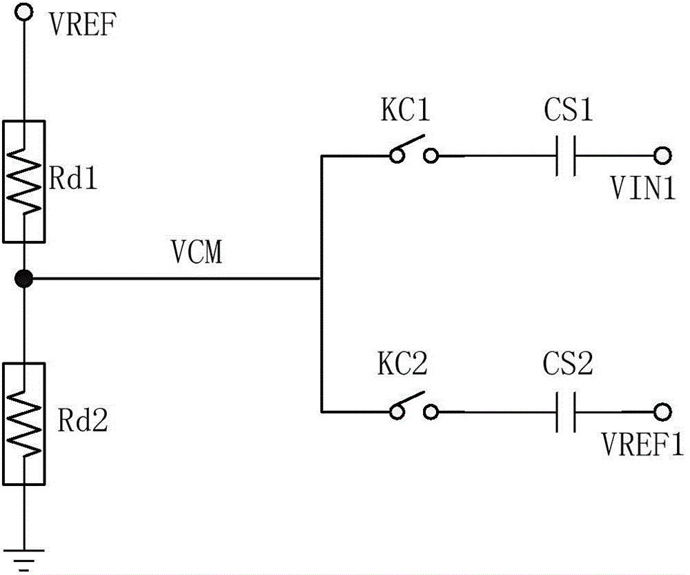
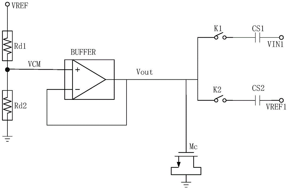
[0064] See image 3 with Figure 4 The first embodiment of the present invention relates to a voltage buffer circuit for driving a load. It should be noted that the illustrations provided in this embodiment only illustrate the basic idea of ​​the present invention in a schematic way, and the figures only show the components related to the present invention instead of the number, shape, and shape of the components in actual implementation. For...


PUM


Abstract

The invention provides a voltage buffer circuit and a circuit including the voltage buffer circuit to be used for driving loads to be switched along with the time sequence. The voltage buffer circuit is used for driving loads and at least comprises a differential input stage, an output stage and a bias module. The voltage buffer circuit is capable of switching drive capacity provided for the loads rapidly, small in power consumption and fast in work speed; the high driving current can be provided when large loads are needed to be driven, the low driving current is provided when large loads are not needed to be driven, the bias module maintains a high current branch in the output stage at a cut-off critical point, and accordingly, the output stage static current is reduced greatly. Meanwhile, the large current branch in the output stage is not cut off completely, so that the large current branch can be connected rapidly when the high driving current is needed, and the circuit switching speed and the reference voltage stability are improved.

Description

technical field [0001] The invention relates to the technical field of snubber circuits, in particular to a voltage snubber circuit and a circuit for sequentially switching driving loads thereof. Background technique [0002] In analog integrated circuits, it is often encountered that the size of the load driven by the reference voltage will switch in time, for example, in SAR ADC (Successive Approximation Register Analog-to-Digital Converter, successive approximation register analog-to-digital converter), the comparator The common-mode reference voltage at the input terminal needs to drive a large sampling capacitor (that is, a load) under the cooperation of timing, so the circuit that provides the common-mode reference voltage plays a key role in the performance of the entire circuit. [0003] In the sampling stage of the SAR ADC circuit, the common-mode reference voltage generated by the reference input voltage needs to be able to quickly drive the large capacitor array t...

Claims


Application Information

Patent Timeline
IPC IPC(8): H03K19/094
Inventor 曹帆程冠楚邢文俊刘军
Owner VERISILICON MICROELECTRONICS SHANGHAI
Why Eureka
Try Eureka