Plasma processing cavity, gas spraying head and manufacturing method thereof

A gas shower head and plasma technology, which is used in the manufacture of semiconductor/solid-state devices, electrical components, discharge tubes, etc., can solve the problems of gas shower head cracking, etc., and achieves low manufacturing cost, dense corrosion-resistant layer and stable structure. reliable results

Active Publication Date: 2015-06-17
ADVANCED MICRO FAB EQUIP INC CHINA
View PDF5 Cites 17 Cited by
  • Summary
  • Abstract
  • Description
  • Claims
  • Application Information

AI Technical Summary

Problems solved by technology

Because the lower surface of the gas shower head is directly exposed to the plasma, it is often necessary to install an anti-corrosion layer on it. However, as the use time increases, the gas shower head often has problems such as cracking

Method used


Image

  • Plasma processing cavity, gas spraying head and manufacturing method thereof
  • Plasma processing cavity, gas spraying head and manufacturing method thereof
  • Plasma processing cavity, gas spraying head and manufacturing method thereof

Examples


Embodiment Construction

[0027] The specific embodiments of the present invention will be described below in conjunction with the accompanying drawings.

[0028] It should be pointed out that the words "semiconductor process piece", "wafer" and "substrate" will often be used interchangeably in the following description, and in the present invention, they all refer to the process processed in the processing chamber. The process parts are not limited to wafers, substrates, substrates, large-area flat substrates, etc. For the convenience of description, the "substrate" will be used as an example in the description and illustrations of the embodiments herein.

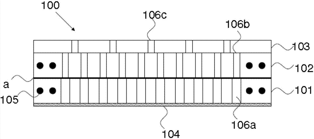
[0029] figure 1 It is a structural schematic diagram of a gas shower head of a plasma processing chamber in the prior art. Such as figure 1 As shown, the showerhead 100 includes a mounting substrate 103 , a second body 102 , a first body 101 , and an yttrium oxide coating 104 from top to bottom. Wherein, the first main body 101 is provided with...


PUM


Abstract

The invention provides a plasma processing cavity, a gas spraying head and a manufacturing method thereof. The gas spraying head is integrally molded and is provided with a plurality of gas through holes machined at a time, and the outer wall of the gas spraying head and inner walls of the gas through holes are each covered with a first anti-corrosion layer. The plasma processing cavity and the gas spraying head are simple in process, and low in manufacturing cost. The gas spraying head is more stable and more reliable in structure; in addition, the anti-corrosion layers are free of pores, are denser and will not crack. The manufacturing process of a base sheet of the plasma processing cavity is more stable.

Description

technical field [0001] The invention relates to the field of semiconductor manufacturing, in particular to a plasma processing chamber, a gas shower head and a manufacturing method thereof. Background technique [0002] The plasma processing device uses the working principle of the vacuum reaction chamber to process the semiconductor substrate and the substrate of the plasma flat panel. The working principle of the vacuum reaction chamber is to pass a reaction gas containing an appropriate etchant source gas into the vacuum reaction chamber, and then input radio frequency energy to the vacuum reaction chamber to activate the reaction gas to stimulate and maintain the plasma, so that The material layer on the surface of the substrate is respectively etched or deposited on the surface of the substrate, and then the semiconductor substrate and the plasma plate are processed. [0003] The gas shower head is an important part of the plasma processing device. One or more gas sou...

Claims


Application Information

Patent Timeline
Patent Type & Authority Applications(China)
IPC IPC(8): H01J37/32H01L21/67
CPCH01J37/3244
Inventor 贺小明徐朝阳彭帆
Owner ADVANCED MICRO FAB EQUIP INC CHINA
Why Eureka
Try Eureka