Gate Forming Method

A gate and pattern technology, applied in the direction of semiconductor devices, etc., can solve the problem of increasing the design value

Active Publication Date: 2017-10-03
SEMICON MFG INT (SHANGHAI) CORP
View PDF3 Cites 0 Cited by
  • Summary
  • Abstract
  • Description
  • Claims
  • Application Information

AI Technical Summary

Problems solved by technology

[0004] However, in the existing method of forming gates, when the gates are cut off, the distance between the disconnected strip gates in the butt direction tends to increase compared with the design value.

Method used


Image

  • Gate Forming Method
  • Gate Forming Method
  • Gate Forming Method

Examples


Embodiment Construction

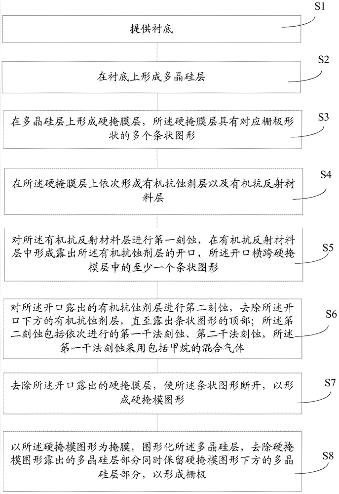
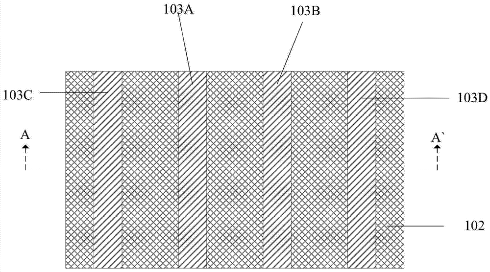
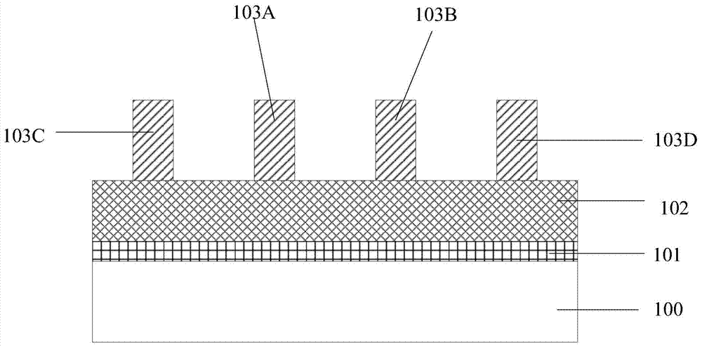
[0029] In the design of narrowing the connecting direction of the gates, the strip-shaped gates are cut by two photolithography steps, but the spacing in the connecting direction of the finally formed and disconnected strip-shaped gates is larger than the designed value.

[0030] In order to obtain the reason why the pitch of the butt joint direction of the strip-shaped gates is larger than the design value, the process of gate cutting in the prior art is analyzed. In the prior art, the dielectric layer usually includes a top-down organic anti-reflective material layer and an organic resist layer. When etching the dielectric layer to form openings, chlorine gas or hydrogen bromide is usually used to etch the organic resist layer. , so that the opening exposes the top of the stripe pattern in the hard mask layer, but the anisotropy of etching with chlorine or hydrogen bromide is poor, and if the etch intensity is low, the organic resist located above the stripe pattern Residue ...


PUM


Abstract

A method for forming a gate, comprising: forming a polysilicon layer on a substrate, forming a hard mask layer having a stripe pattern corresponding to the gate shape on the polysilicon layer, and sequentially forming an organic resistive layer on the hard mask layer. The etchant layer and the organic anti-reflection material layer, the first etching is performed on the organic anti-reflection material layer to form an opening, and the second etching is performed on the organic resist layer exposed by the opening to expose the strip-shaped opening. graphics. In the second etching process, the first dry etching and the second dry etching using a mixed gas including methane are sequentially performed, wherein the first dry etching uses methane as the etching gas, and the first dry etching The lateral etching of the organic anti-reflective material layer is very little, which alleviates the problem of increasing the size of the opening, and then etches the hard mask layer under the opening, so that the finally formed disconnected strip-shaped gate Compared with the design value, the spacing in the butt direction of the poles increases very little.

Description

technical field [0001] The invention relates to the field of semiconductor manufacturing, in particular to a method for forming a grid. Background technique [0002] Poly Cut technology is used to cut off the strip gate, and the cut gate corresponds to different transistors, which can improve the integration of transistors. In addition, when a plurality of gates are arranged in a row along the extending direction, the pitch in the butting direction between gates that are disconnected after gate cutting can be narrowed with high precision by gate cutting (Poly Cut CD). [0003] In the existing gate cutting process, a polysilicon layer is usually formed on the substrate first, and then a patterned hard mask layer is formed on the surface of the polysilicon layer. The patterned hard mask layer has bar graph. In order to cut off the striped gates, it is necessary to form a patterned photoresist layer on the hard mask layer above the striped pattern, and the patterned photoresi...

Claims


Application Information

Patent Timeline
Patent Type & Authority Patents(China)
IPC IPC(8): H01L21/28
Inventor 韩秋华孟晓莹
Owner SEMICON MFG INT (SHANGHAI) CORP
Why Eureka
Try Eureka