P-type buried layer covered superjunction lateral double diffused metal oxide semiconductor field effect transistor
An oxide semiconductor, lateral double diffusion technology, applied in semiconductor devices, electrical components, circuits, etc., can solve the problems of reducing SJ-LDMOS breakdown voltage, low specific on-resistance, high breakdown voltage, etc.
- Summary
- Abstract
- Description
- Claims
- Application Information
AI Technical Summary
Problems solved by technology
Method used
Image
Examples
Embodiment Construction
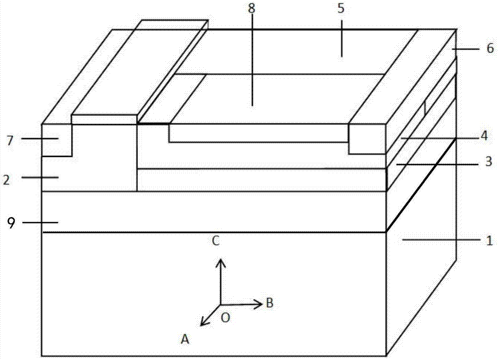
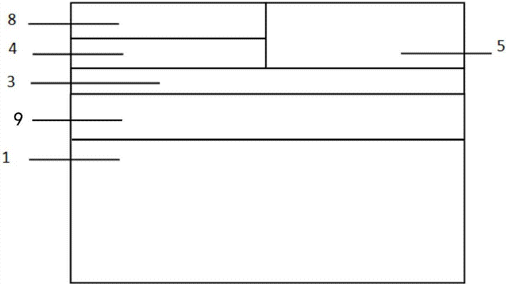
[0028] see figure 1 and figure 2 In the following, a P-type buried layer-covered N-channel superjunction lateral double-diffused metal-oxide-semiconductor field-effect transistor is used as an example to specifically introduce the new structure in the embodiment of the present invention:
[0029] P-type buried layer covered N-channel super-junction lateral double-diffused metal oxide semiconductor field effect transistor, including:
[0030] P-type semiconductor substrate 1;
[0031] The P-type base region 2 and the N-type buffer layer 3 adjacent to the surface of the N-type epitaxial layer 9 on the P-type semiconductor substrate;
[0032] The super junction region adjacent to the P-type base region on the N-type buffer layer 3 includes N-type pillar regions 4 and P-type pillar regions 5 arranged laterally and periodically;
[0033] The P-type doped buried layer 8 located on the N-type pillar region 4 and only adjacent to the N-type drain region 6 has an N-type drift regio...
PUM
 Abstract
Description
Claims
Application Information

