

Pseudo gate removing method
A dummy gate and dry cleaning technology, which is applied in the direction of electrical components, semiconductor/solid-state device manufacturing, semiconductor devices, etc., can solve problems such as damage and poor insulation, and achieve improved performance, good shape, and repair of titanium nitride capping layer Effect
- Summary
- Abstract
- Description
- Claims
- Application Information
AI Technical Summary
Problems solved by technology
Method used
Image

Examples
Embodiment Construction
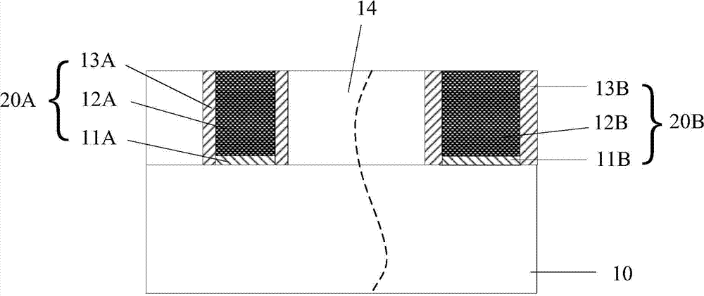
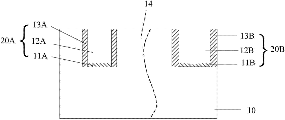
[0029] In the existing methods for removing dummy gates, dry etching is usually used to remove dummy gates, but the removal rates of dummy gates of different sizes are different when dry etching is used to remove dummy gates. The removal rate of dummy gate is faster, but the removal rate of dummy gate with smaller size is slower. When the smaller dummy gate is removed, the gate dielectric layer under the larger dummy gate is easily damaged due to premature exposure. After the dummy gate is removed and the metal gate is filled in the opening, the metal gate The insulation between the transistor and the substrate is poor. When the transistor is an NMOS, damage to the gate dielectric layer will seriously affect the time-dependent breakdown characteristics (Time Dependent Dielectric Breakdown, TDDB) of the NMOS.
[0030] Analyzing the process of removing the dummy gate, for a dummy gate with a larger size, the opening formed on the surface of the dummy gate at the beginning of etc...
PUM
 Abstract
Description
Claims
Application Information