

Method of preparing on-insulator material with accurate and controllable stripping position
An insulator and precise technology, which is applied in the field of preparation of materials on insulators, can solve the problems of rough peeling surface, inaccurate control of peeling position, large implantation dose, etc., and achieve the goal of reducing damage, small ion implantation dose, and precise control of peeling position Effect
- Summary
- Abstract
- Description
- Claims
- Application Information
AI Technical Summary
Problems solved by technology
Method used
Image

Examples
Embodiment 1
[0046] Such as Figure 1 to Figure 6 As shown, the present invention provides a method for preparing a material on an insulator with precise and controllable peeling positions, which at least includes the following steps:
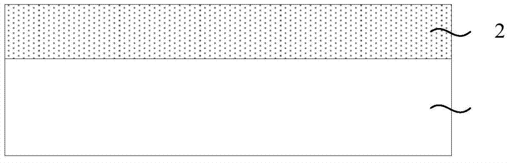
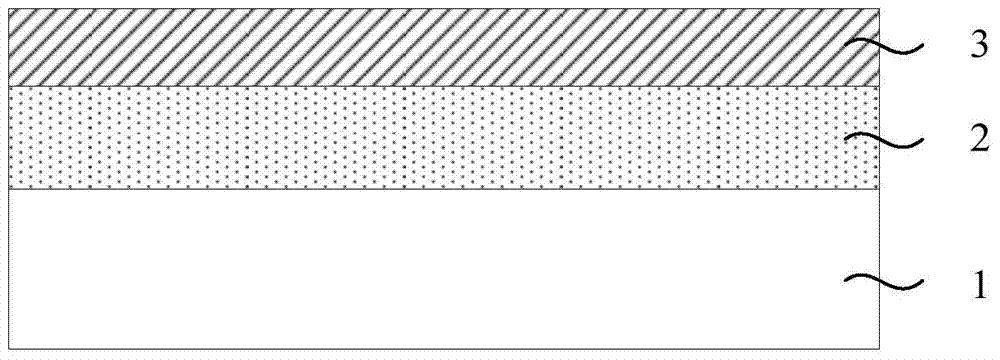
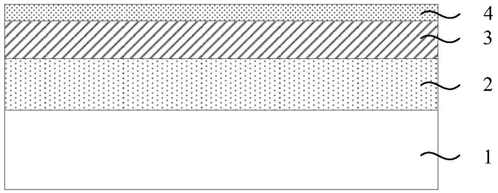
[0047] S1: Provide a Si substrate, and epitaxially grow a doped single crystal layer on the surface of the Si substrate; the thickness of the doped single crystal layer is greater than 15 nm;
[0048]S2: epitaxially growing a single crystal thin film on the surface of the doped single crystal layer;
[0049] S3: forming a SiO on the surface of the single crystal thin film 2 Floor;
[0050] S4: from the SiO 2 Ion implantation is performed on the front side of the layer so that the ion peaks are distributed in the SiO 2 Within the preset range below the layer;
[0051] S5: Provide a substrate with an insulating layer on the surface, combine the insulating layer on the surface of the substrate with the SiO on the surface of the single crystal thin film 2...
Embodiment 2
[0070] This embodiment adopts basically the same technical solution as that of Embodiment 1, except that the ion implantation position is different from the stripping position.
[0071] See first Figure 1 to Figure 3 , and perform steps S1 to S3 that are basically the same as those in Embodiment 1. For details, refer to Embodiment 1, which will not be repeated here.
[0072] then see Figure 7 , execute step S4: from the SiO 2 Ion implantation is performed on the front side of layer 4 so that the ion peaks are distributed in the SiO 2 Within the preset range below layer 4.
[0073] Specifically, H, He or H / He is used for ion implantation, and the ion implantation dose ranges from 1E16 to 5E16 cm -2 . In this embodiment, H element is preferably used for ion implantation, and the implantation dose is 3E16cm -2 .
[0074] In this embodiment, by controlling the implantation energy E to satisfy 21keV
Embodiment 3
[0083] This embodiment adopts basically the same technical solution as that of Embodiment 1, except that the ion implantation position is different from the stripping position.
[0084] See first Figure 1 to Figure 3 , and perform steps S1 to S3 that are basically the same as those in Embodiment 1. For details, refer to Embodiment 1, which will not be repeated here.
[0085] then see Figure 10 , execute step S4: from the SiO 2 Ion implantation is performed on the front side of layer 4 so that the ion peaks are distributed in the SiO 2 Within the preset range below layer 4.
[0086] Specifically, H, He or H / He is used for ion implantation, and the ion implantation dose ranges from 1E16 to 5E16 cm -2 . In this embodiment, H element is preferably used for ion implantation, and the implantation dose is 3E16cm -2 .
[0087] In this embodiment, by controlling the implantation energy E to satisfy 10keV
PUM
| Property | Measurement | Unit |
|---|---|---|
| thickness | aaaaa | aaaaa |
| thickness | aaaaa | aaaaa |
| thickness | aaaaa | aaaaa |
Abstract
Description
Claims
Application Information