AC-DC (alternating current-direct current) drive output filter capacitor quick active leakage circuit
An output filtering and bleeder circuit technology, applied in the field of electronics, can solve the problems of aggravating the internal temperature rise of the driving power supply, low reliability and practicability, and affecting the efficiency of the power supply, so as to achieve low power consumption, prevent overcurrent damage and discharge. Current controllable effect
- Summary
- Abstract
- Description
- Claims
- Application Information
AI Technical Summary
Problems solved by technology
Method used
Image
Examples
Embodiment 1
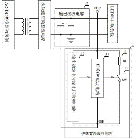
[0033] see figure 1 , is a schematic block diagram of an AC-DC driver output filter capacitor fast active discharge circuit provided by the present invention.
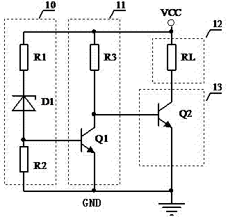
[0034] The AC-DC driver output filter capacitor fast active discharge circuit includes: output filter capacitor terminal voltage detection circuit 10, switch SW drive circuit 11, switch SW13 and low resistance load resistor RL12, the positive terminal of the fast active discharge circuit VCC is connected to the positive pole of the output filter capacitor 2 of the AC-DC converter, the negative terminal GND of the fast active discharge circuit is connected to the negative pole of the output filter capacitor 2 of the AC-DC converter, the low-impedance load resistor RL12 is connected in series with the switch SW13, and the load resistor One end of R12L is connected to the positive terminal VCC of the fast active discharge circuit, the other end is connected to the switch SW13, and the other end of the switch SW13 is conne...
Embodiment 2
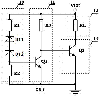
[0039] For the convenience of the selection of the discharge voltage, in the second implementation of the AC-DC driver output filter capacitor fast active discharge circuit of the present invention, as image 3 As shown, two zener diodes D11 and D12 in series in the same direction are used to form the discharge voltage detection element, that is, the zener diode D1 in the first embodiment is replaced by two zener diodes D11 and D12 in series in the same direction. Other structures of the second embodiment are the same as those of the first embodiment, and will not be repeated here.
Embodiment 3
[0041] Such as Figure 4 As shown, on the basis of Embodiment 2, considering that the current amplification factor β of the single power NPN transistor Q2 is limited, use NPN transistors Q21 and Q22 to form a composite tube with a high current amplification factor instead of the single power NPN transistor Q2 as the switch SW12, To increase the current amplification factor β of the switch SW, so as to further increase the resistance value of the collector load resistor R3 and the current limiting resistor R1, and further reduce the power consumption of the active discharge circuit, wherein the collectors of the NPN transistors Q21 and Q22 and connected together, and connected to one end of the load resistor RL12, the emitter of the NPN transistor Q21 is connected to the base of the NPN transistor Q22. In addition, a resistor R5 is introduced into the switch SW13, one end of the resistor R5 is connected to the emitter of the NPN transistor Q21 and the base of the NPN transistor...
PUM
 Abstract
Description
Claims
Application Information


