

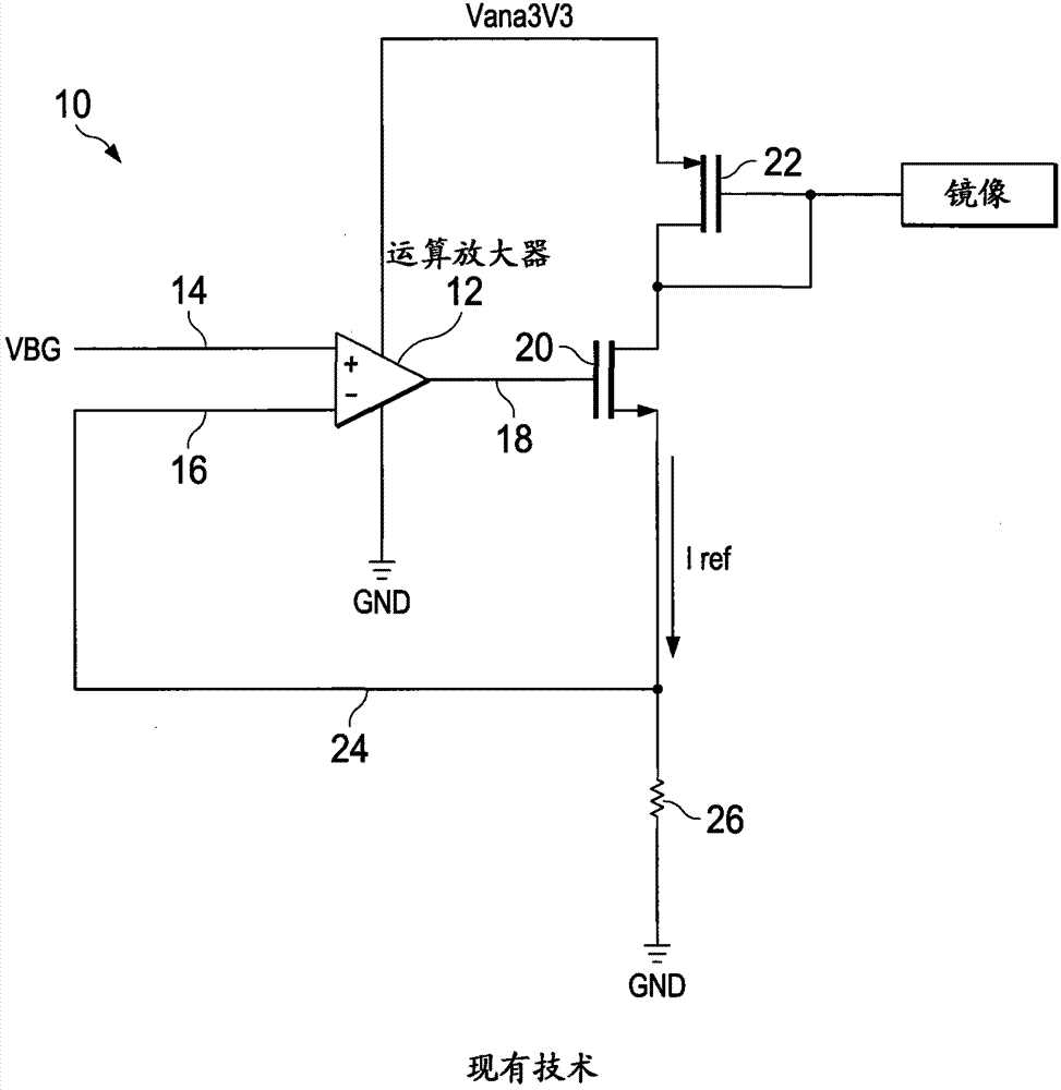
Current reference circuit for temperature and process compensation
A technology for generating reference current and reference voltage, which is applied in the direction of adjusting electrical variables, control/regulation systems, instruments, etc., and can solve problems such as errors
- Summary
- Abstract
- Description
- Claims
- Application Information
AI Technical Summary
Problems solved by technology
Method used
Image

Examples
Embodiment Construction
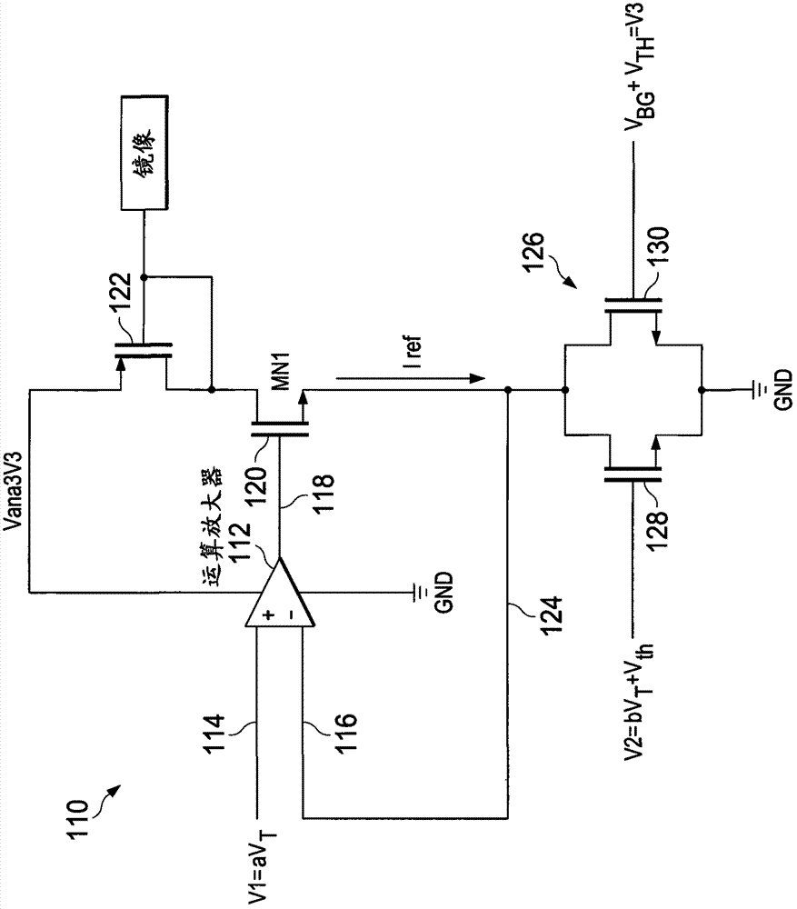
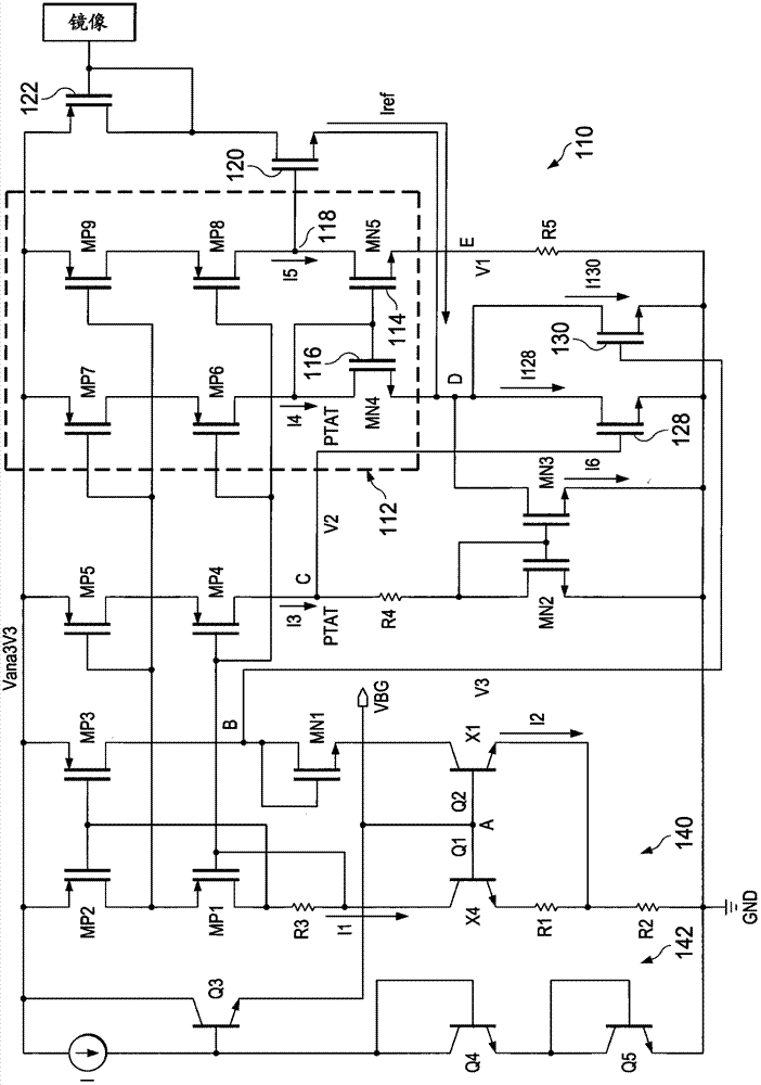
[0017] now refer to figure 2 , which illustrates a circuit diagram of an embodiment of a temperature and process compensated reference current generator circuit 110 . Circuit 110 includes an operational amplifier 112 having a non-inverting (positive) input 114 and an inverting (negative) input 116 . The non-inverting input terminal 114 is configured to receive a first reference voltage V1=aV T . In this case, V T =kT / q is known to those skilled in the art and a is a scaling constant set by the circuit designer for the reference voltage generator. Amplifier 112 is powered from positive and negative voltage supply nodes, in this case as indicated by voltage Vana3V3 (eg, an analog circuit supply voltage of 3V) and ground. The amplifier includes an output node 118 coupled to the gate of transistor 120 . Transistor 120 is an n-channel MOSFET device. The source-drain path of transistor 120 is coupled between a positive voltage supply node and a negative voltage supply node. ...
PUM
 Abstract
Description
Claims
Application Information