A method of manufacturing a circuit board

A manufacturing method and circuit board technology, which is applied in the direction of printed circuit manufacturing, printed circuit, electrical components, etc., can solve the problems of circuit board shape deviation, difficult to design positioning holes, and small-sized circuit boards are difficult to fix, so as to improve production Efficiency and pass rate, improvement of inspection efficiency and accuracy, and the effect of reducing the number of scratches

Active Publication Date: 2017-08-11
GCI SCI & TECH
View PDF6 Cites 0 Cited by
  • Summary
  • Abstract
  • Description
  • Claims
  • Application Information

AI Technical Summary

Problems solved by technology

However, due to the small area of ​​the small-sized circuit board, it is difficult to design positioning holes in the board, which makes it difficult to fix the small-sized circuit board during the shape processing process, resulting in problems such as deviation and damage of the circuit board shape
Moreover, if the size of the circuit board is smaller than the dust suction device of the processing equipment, it is easy to be sucked away by the dust suction device during processing.
[0004] In addition, when inspecting small-sized circuit boards, due to the small size of the board, it is inconvenient for the inspector to take it, thereby reducing the inspection efficiency. Cause problem board to flow out

Method used


Image

  • A method of manufacturing a circuit board
  • A method of manufacturing a circuit board
  • A method of manufacturing a circuit board

Examples


Embodiment Construction

[0029] The following will clearly and completely describe the technical solutions in the embodiments of the present invention with reference to the accompanying drawings in the embodiments of the present invention. Obviously, the described embodiments are only some, not all, embodiments of the present invention. Based on the embodiments of the present invention, all other embodiments obtained by persons of ordinary skill in the art without creative efforts fall within the protection scope of the present invention.

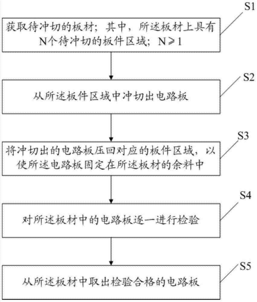
[0030] see figure 1 , is a schematic flow diagram of an embodiment of the method for manufacturing a circuit board provided by the present invention, including:

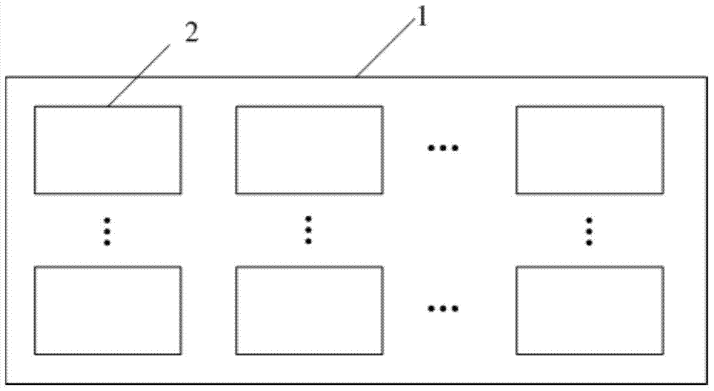
[0031] S1. Obtain the plate to be punched; wherein, there are N plate areas to be punched on the plate; N≥1;

[0032] S2, punching out a circuit board from the board area;

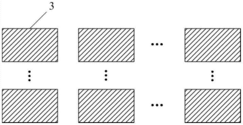
[0033] S3. Press the punched circuit board back to the corresponding plate area, so that the circuit board is fixed in the remaini...


PUM


Abstract

The invention discloses a method for manufacturing a circuit board, comprising: obtaining a plate to be punched; wherein, the plate has N plate areas to be punched; N≥1; punching from the plate area Cutting out the circuit board; pressing the punched out circuit board back to the corresponding panel area so that the circuit board is fixed in the remaining material of the panel; inspecting the circuit boards in the panel one by one; Take out the qualified circuit board from the board. By adopting the embodiment of the present invention, the production efficiency and inspection accuracy of the circuit board can be improved.

Description

technical field [0001] The invention relates to the technical field of printed circuit boards, in particular to a method for manufacturing a circuit board. Background technique [0002] With the development of PCB (Printed Circuit Board, printed circuit board) towards the direction of small size, light weight, three-dimensional installation and high connection reliability, more and more small size boards are used in the PCB industry. Shape processing and finished product inspection are two essential processes in the circuit board manufacturing process. Among them, the shape processing is specifically to use the shape processing equipment (such as punching machine, edge milling machine) to process the imposition products into the form of veneer or delivery panel required by customers; the inspection of finished products is to use the finished circuit boards before shipment Check the quality of the board surface with naked eyes or borrow tools (such as magnifying glass, etc.)...

Claims


Application Information

Patent Timeline
Patent Type & Authority Patents(China)
IPC IPC(8): H05K3/00
Inventor 任安源黄德业李超谋任代学刘俊
Owner GCI SCI & TECH
Why Eureka
Try Eureka