Manufacturing method of small-size circuit boards

A manufacturing method and circuit board technology, applied in the field of printed circuit boards, can solve the problems of difficult design of positioning holes for boards, deviation of circuit board shape, and difficulty in fixing small-sized circuit boards, so as to improve inspection efficiency and accuracy, improve Production efficiency and yield, and the effect of reducing the number of scratches

Inactive Publication Date: 2019-04-05
江门市利诺达电路科技有限公司
View PDF5 Cites 0 Cited by
  • Summary
  • Abstract
  • Description
  • Claims
  • Application Information

AI Technical Summary

Problems solved by technology

[0003] In the prior art, the shape of the small-sized circuit board is processed by milling machine technology. However, due to the small area of ​​the small-sized circuit board, it is difficult to design positioning holes in the board, which makes it difficult to fix the small-sized circuit board during the process of shape processing, resulting in Problems such as deviation and breakage of the circuit board shape; moreover, when the size of the circuit board is smaller than the dust col

Method used


Image

  • Manufacturing method of small-size circuit boards
  • Manufacturing method of small-size circuit boards
  • Manufacturing method of small-size circuit boards

Examples


Embodiment Construction

[0032] The following will clearly and completely describe the technical solutions in the embodiments of the present invention with reference to the accompanying drawings in the embodiments of the present invention. Obviously, the described embodiments are only some, not all, embodiments of the present invention. Based on the embodiments of the present invention, all other embodiments obtained by persons of ordinary skill in the art without creative efforts fall within the protection scope of the present invention.

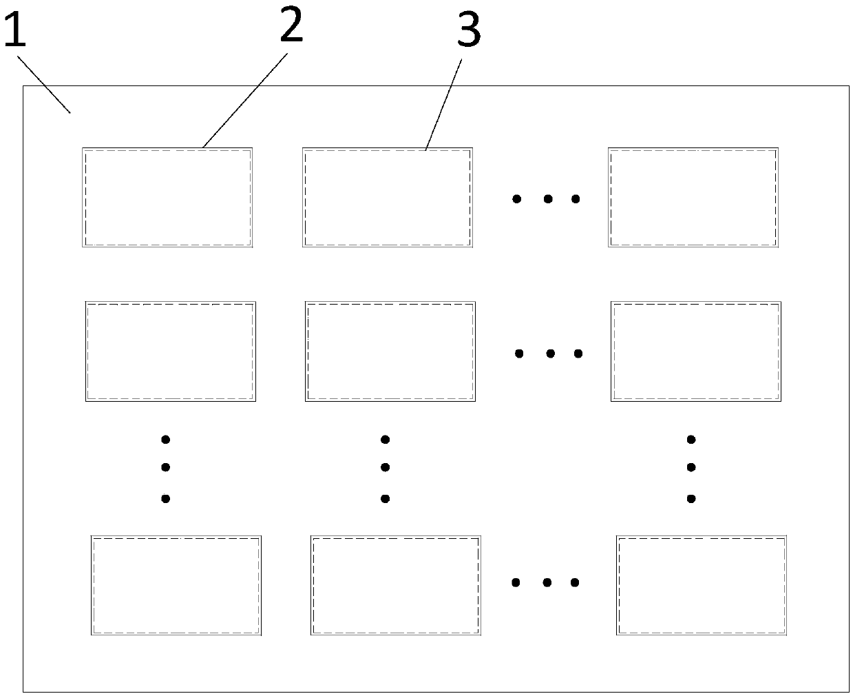
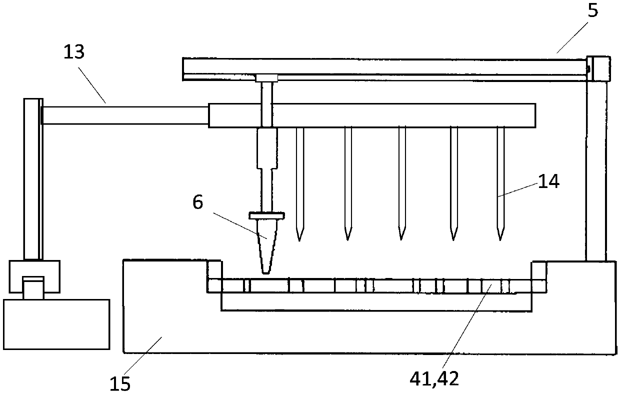
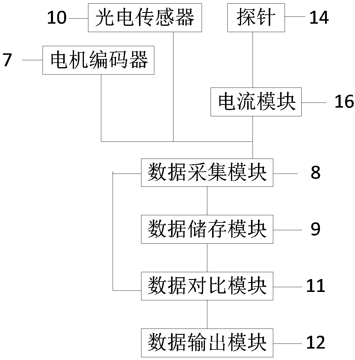
[0033] Such as Figure 1 to Figure 3 As shown, the preferred embodiment of the present invention, a method for making a small-sized circuit board, includes the following processes: cutting, drilling, copper sinking, pattern transfer, pattern electroplating, film removal, etching, green oil, characters, gold plating Finger, molding and testing, it is characterized in that, the specific steps of described molding and described testing are as follows:

[0034] S1: Ob...


PUM


Abstract

The invention provides a manufacturing method of small-size circuit boards. The manufacturing method comprises the steps: forming is conducted, specifically, through the design of cutting lines, the circuit boards can still be connected into boards after being subjected to blanking forming, especially for manufacturing of the small-size circuit boards, positioning holes do not need to be designedin all the circuit boards, thus shape damage of the circuit boards is reduced, the production efficiency of the circuit boards is improved, and the yield of the circuit boards is increased; and detecting is conducted, specifically, hole quality detection is conducted on the circuit boards one by one firstly, the quality, in the aspects of hole position, hole diameter, hole blocking condition and the like, of via holes can be judged firstly by comparing the difference of the illumination intensity, detected by a photoelectric sensor, of a light source passing through the standard holes and theto-be-detected holes, then the quality of all loops of the circuit boards is detected, and the short circuit situation of all the loops of the to-be-detected circuit boards is judged by comparing thedifference of inductance values, detected by a probe, of all the loops of the standard circuit boards and all the loops of the to-be-detected circuit boards. The manufacturing method has the advantages of convenient machining, high production efficiency, high detecting efficiency, accurate detecting and high checking efficiency.

Description

technical field [0001] The invention relates to the technical field of printed circuit boards, in particular to a method for manufacturing small-sized circuit boards. Background technique [0002] With the development of circuit boards in the direction of small size, light weight, three-dimensional installation and high connection reliability, there are more and more small-sized circuit boards in the printed circuit board industry. Shape processing and finished product inspection are essential in the process of circuit board production. There are two least processes, among which, the shape processing is specifically to use the shape processing equipment (such as punching machine, edge milling machine) to process the imposition products into the single board form or delivery panel form required by the customer; the finished product inspection is specifically the finished circuit Before the board is shipped, use the naked eye or borrow tools (such as a magnifying glass, etc.) ...

Claims


Application Information

Patent Timeline
IPC IPC(8): G01R31/28G01N21/95
CPCG01N21/95G01R31/2812G01R31/2898
Inventor 童雷童炳武童大望潘世丹
Owner 江门市利诺达电路科技有限公司
Why Eureka
Try Eureka