Self-biased ultra wideband low-power-consumption low-noise amplifier (LNA)

A low-noise amplifier, ultra-wideband technology, applied in the direction of improving amplifiers to expand bandwidth, improving amplifiers to reduce noise effects, and control of amplification, which can solve difficult broadband input matching, difficult to achieve high flat gain, and large chip area. and other problems, to achieve the effect of realizing ultra-wideband power and noise matching, optimizing broadband input power matching, and optimizing high-frequency noise performance

Active Publication Date: 2015-07-15
NO 54 INST OF CHINA ELECTRONICS SCI & TECH GRP
View PDF8 Cites 14 Cited by
  • Summary
  • Abstract
  • Description
  • Claims
  • Application Information

AI Technical Summary

Problems solved by technology

However, the first implementation method will occupy a large chip area, and has high power consumption and poor noise performance; the second method is not easy to achieve wideband input matching; the third method is difficult to achieve high flat g

Method used


Image

  • Self-biased ultra wideband low-power-consumption low-noise amplifier (LNA)
  • Self-biased ultra wideband low-power-consumption low-noise amplifier (LNA)
  • Self-biased ultra wideband low-power-consumption low-noise amplifier (LNA)

Examples


Embodiment Construction

[0017] The present invention will be further described in detail below in conjunction with the accompanying drawings and specific embodiments.

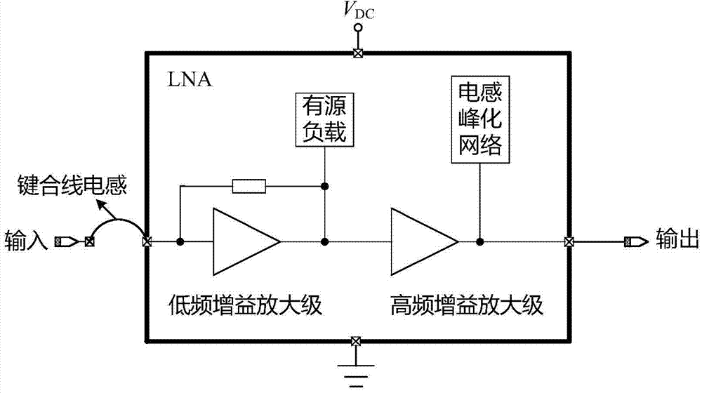
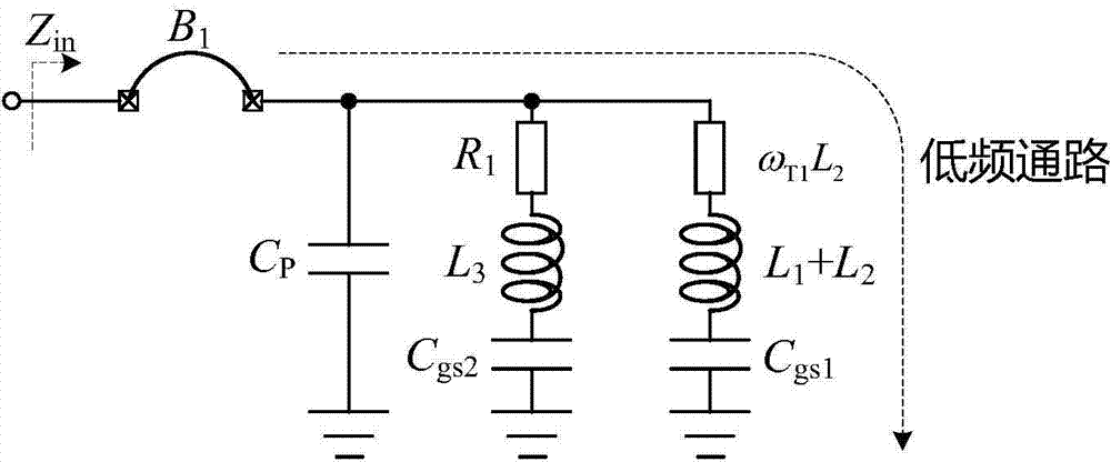
[0018] The LNA of the present invention adopts figure 1 The two-stage cascaded topology is shown. The first stage is a low-frequency gain amplification stage, which uses active devices as loads and resistor negative feedback technology; the second stage is a high-frequency gain amplification stage, which uses a Cascode structure as the basic amplification unit and an inductance peaking network as the load.

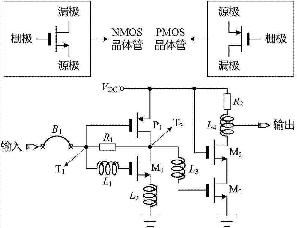
[0019] see figure 2 , the present invention utilizes three NMOS transistors, one PMOS transistor, five passive inductors, and two resistors to realize the circuit design of self-biased ultra-wideband low-power LNA. where the NMOS transistor M 1 , PMOS transistor P 1 , On-chip spiral inductor L 1 , L 2 and resistor R 1 Makes up the first stage of the LNA; NMOS transistor M 2 , M 3 , On-chip spiral inductor L 3 , On-chip ...


PUM


Abstract

The invention provides a self-biased ultra wideband low-power-consumption low-noise amplifier (LNA) and belongs to the field of radio frequency integrated circuits. The LNA only contains a low-frequency amplifier stage and a high-frequency amplifier stage. At the low-frequency amplifier stage of the LNA, an active load is combined with the resistive negative feedback technology to provide bias for a circuit at the same stage and a circuit at a backward stage, self-bias of the overall LNA circuit is achieved, the circuit design is simplified, and circuit power consumption is restrained. According to the structural features of the circuit, and high-frequency matching and noise performance of the circuit are optimized by fully utilizing parasitic inductance of bonding wires. At the high-frequency amplifier stage, the working frequency range of the LNA is expanded through the inductance peaking technology. The LNA can stably work within the frequency range of 0.2-6 GHz, and gain of 16+/-1.3 dB, the noise coefficient smaller than 2-8 dB and good input matching are maintained. The self-biased ultra wideband low-power-consumption LNA can be applied to receiver front-end chips applied to digital broadcasting, wireless local area networks, ultrashort wave radars and other devices.

Description

technical field [0001] The invention belongs to the field of radio frequency integrated circuits, and relates to a low noise amplifier (Low Noise Amplifier, hereinafter referred to as LNA), especially an ultra-wideband low-power LNA without an independent bias circuit and powered by a single power supply. Background technique [0002] Driven by factors such as cost, integration and power consumption, CMOS technology has achieved unprecedented development. The continuous improvement of the cut-off frequency of CMOS transistors has increased the degree of freedom in the design of integrated circuits in frequency bands below a few GHz. With the development of multimedia technology and communication technology, the LNA at the front end of the receiver is expected to work at hundreds of MHz to several GHz to adapt to fields such as wireless local area networks (5GHz (802.11a) and 2.4GHz (802.11b / g)) application requirements. This demand has triggered more attention and research...

Claims


Application Information

Patent Timeline
IPC IPC(8): H03F1/26H03F1/42H03G3/20
Inventor 杨格亮许仕龙杜克明王明魏恒刘长龙吕杰
Owner NO 54 INST OF CHINA ELECTRONICS SCI & TECH GRP
Why Eureka
Try Eureka