Memorizer apparatus and memorizer control method

A control method and memory technology, applied in static memory, read-only memory, digital memory information and other directions, to achieve the effect of eliminating capacitive coupling effects

Active Publication Date: 2015-07-22
WINBOND ELECTRONICS CORP
View PDF3 Cites 0 Cited by
  • Summary
  • Abstract
  • Description
  • Claims
  • Application Information

AI Technical Summary

Problems solved by technology

[0004] The technical problem to be solved by the present invention is to provide a memory device and a memory control method to solv

Method used


Image

  • Memorizer apparatus and memorizer control method
  • Memorizer apparatus and memorizer control method
  • Memorizer apparatus and memorizer control method

Examples


Embodiment Construction

[0038] In order to make the purpose, features and advantages of the present invention more comprehensible, specific embodiments of the present invention are listed below, together with the attached drawings, for detailed description as follows.

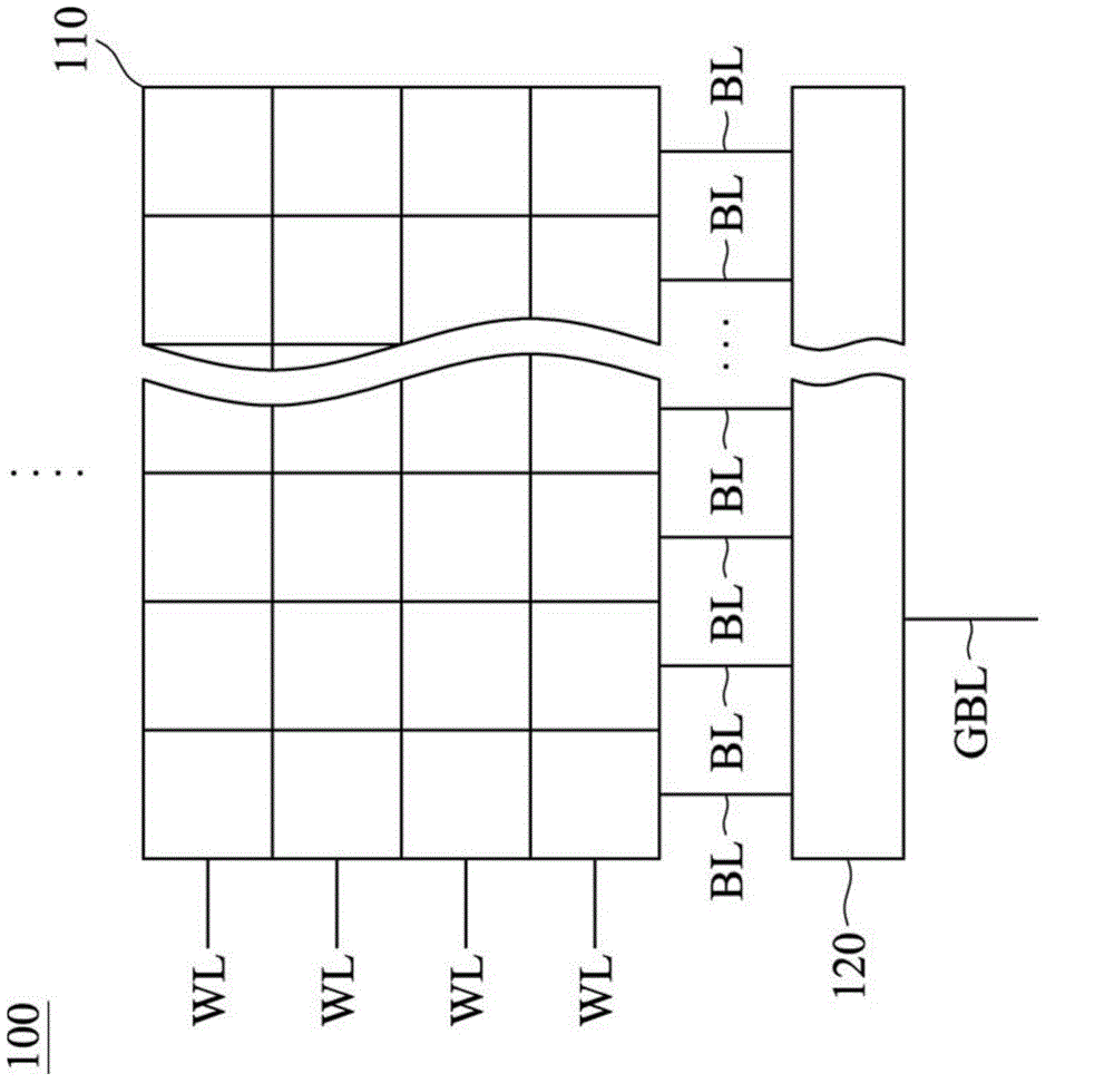
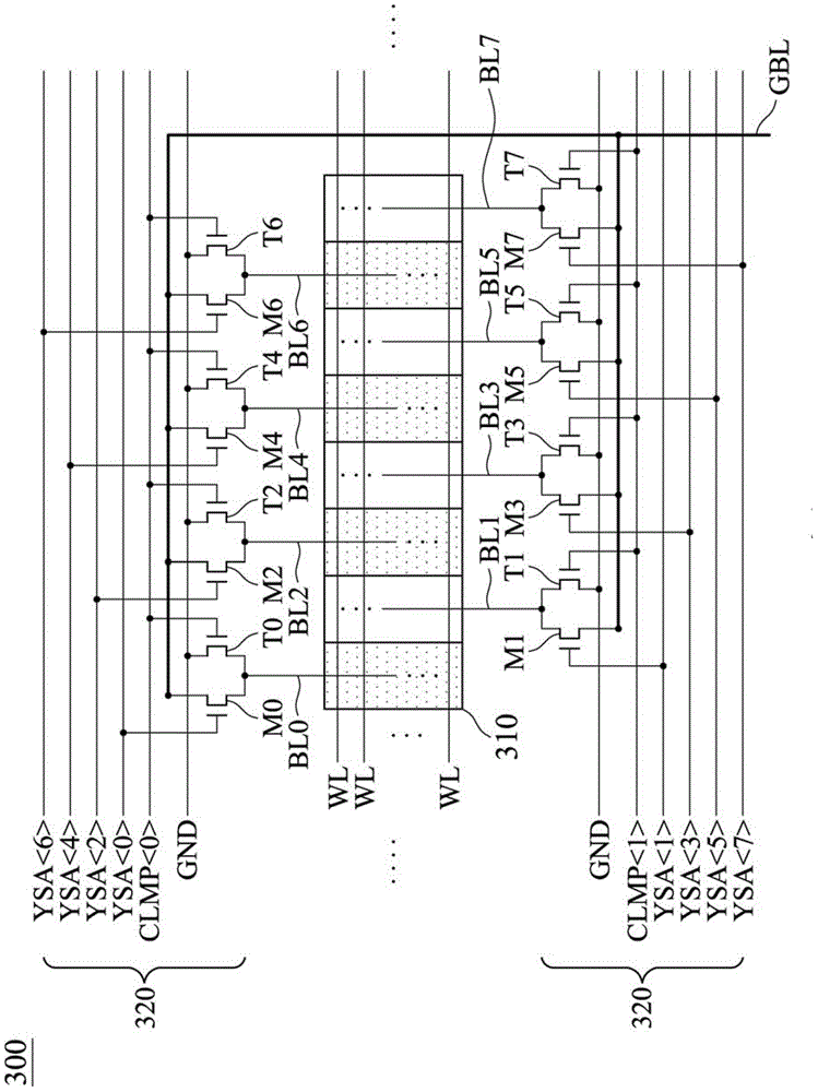
[0039] image 3 A schematic diagram of a memory device 300 according to an embodiment of the invention is shown. The memory device 300 may be a flash memory (Flash Memory), such as a NOR flash memory. Such as image 3 As shown, the memory device 300 includes at least a memory cell array (Memory Cell Array) 310 and a column decoder (Column Decoder) 320 . It must be understood that the memory device 300 may also include other components, such as a driver, a row decoder, and a sense amplifier (SA). To simplify the drawing, some elements of the memory device 300 are omitted and not shown in image 3middle. The memory cell array 310 may include a plurality of memory cells (Memory Cell). In some embodiments, the memory cell array 310 ...


PUM


Abstract

The invention discloses a memorizer apparatus and a memorizer control method. The memorizer apparatus comprises a memory cell array and a column decoder; the memory cell array comprise a plurality of even local bit lines, and a plurality of odd local bit lines; the column decoder comprises a plurality of even channel transistors, a plurality of even clamped transistors, a plurality of odd channel transistors, and a plurality of odd clamped transistors; the control terminal of each even clamped transistor is connected with an even clamped wire via coupling connection; the first terminal of each even clamped transistor is connected with one independent even local bit line via coupling connection; the second terminal of each even clamped transistor is connected with a ground potential via coupling connection; the control terminal of each odd clamped transistor is connected with an odd clamped wire via coupling connection; the first terminal of each odd clamped transistor is connected with one independent odd local bit line via coupling connection; and the second terminal of each odd clamped transistor is connected with the ground potential via coupling connection. The memorizer apparatus is capable of eliminating capacitive coupling effect between adjacent memory cells effectively.

Description

technical field [0001] The present invention relates to a memory device, in particular to a memory device with a column decoder, wherein the column decoder can be used to reduce the capacitive coupling effect between adjacent memory cells. Background technique [0002] figure 1 is a schematic diagram showing a conventional memory device 100 . Such as figure 1 As shown, the memory device 100 includes at least a memory cell array (Memory Cell Array) 110 and a column decoder (Column Decoder) 120 . To simplify the drawing, the remaining elements of the memory device 100 are omitted and not shown in figure 1 middle. The memory cell array 110 includes a plurality of memory cells (Memory Cell). A plurality of word lines (Word Line) WL and a plurality of local bit lines (Local Bit Line) BL can be used to select these memory cells. In addition, the column decoder 120 can be used to selectively couple one of the local bit lines BL to a global bit line (Global Bit Line) GBL. [...

Claims


Application Information

Patent Timeline
IPC IPC(8): G11C11/40G11C16/06
Inventor 河壬喆苏仁福
Owner WINBOND ELECTRONICS CORP
Why Eureka
Try Eureka