
Novel high-area-efficiency and low-triggering silicon controlled

An area-efficient, low-voltage triggering technology, applied in electrical components, electrical solid-state devices, circuits, etc., can solve problems such as large single area and not meeting high area efficiency requirements, and achieve strong positive feedback and maximum current discharge capability. , the effect of high area efficiency

Inactive Publication Date: 2015-07-29
江苏艾伦摩尔微电子科技有限公司
View PDF4 Cites 3 Cited by
  • Summary
  • Abstract
  • Description
  • Claims
  • Application Information

AI Technical Summary

Problems solved by technology

Conventional low-voltage trigger thyristors often have a large single area, which does not meet the requirements of high area efficiency

Method used


Image

  • Novel high-area-efficiency and low-triggering silicon controlled
  • Novel high-area-efficiency and low-triggering silicon controlled

Examples


Embodiment Construction

[0013] The present invention will be further described below in conjunction with the accompanying drawings.

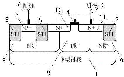
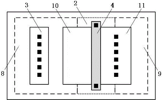
[0014] Such as figure 1 , figure 2 As shown, a new high-area efficiency low-voltage trigger thyristor, including P-type substrate 1, N well, P well 2, also includes P+ implantation region 3, N+ implantation region, polysilicon gate 4, shallow trench isolation 5, Cathode 6, anode 7, described N well comprises first N well 8, second N well 9, described N+ implantation region comprises first N+ implantation region 10, second N+ implantation region 11, described P-type substrate 1 The first N well 8, the P well 2, and the second N well 9 are sequentially arranged along the upper horizontal direction; the P+ implantation region 3 is arranged on the first N well 8, and the first N+ implantation region 10 is arranged across the first N well. On the N well 8 and the P well 2, the second N+ implantation region 10 straddles the P well 2 and the second N well 9; the polysilico...


PUM


Abstract

The invention discloses a novel high-area-efficiency and low-triggering silicon controlled. The novel high-area-efficiency and low-triggering silicon controlled comprises a P type substrate, an N trap, a P trap, a P<+> injection domain, a polysilicon gate, a shallow-trench isolator, a cathode and an anode; the N trap comprises a first N trap and a second N trap; the N<+> injection domain comprises a first N<+> injection area and a second N<+> injection domain; the first N trap, the P trap and the second N trap are sequentially transversely arranged on the P type substrate; the P<+> injection domain is arranged on the first N trap; the first N<+> injection domain is arranged cross the first N trap and the P trap; the second N<+> injection domain is arranged cross the P trap and the second N trap; the polysilicon gate is arranged on the P trap; the P<+> injection domain is connected with the anode; the polysilicon gate and the second N<+> injection domain are connected with the cathode. According to the novel high-area-efficiency and low-triggering silicon controlled, the P<+> injection domain, the first N trap, the P trap and the second N<+> injection domain are used to achieve a silicon controlled path, so that the area efficiency is high; the whole protection device is simple in structure, stable and reliable.

Description

technical field [0001] The invention relates to a novel low-voltage trigger thyristor with high area efficiency and belongs to the technical field of integrated circuits. Background technique [0002] The phenomenon of electrostatic discharge (ESD) in nature poses a serious threat to the reliability of integrated circuits. In the industry, 37% of the failures of integrated circuit products are caused by electrostatic discharge. Moreover, with the increasing density of integrated circuits, on the one hand, due to the thinner and thinner silicon dioxide film (from micron to nanometer), the electrostatic pressure on the device is getting lower and lower; on the other hand, it is easy to generate and accumulate The extensive use of electrostatic materials such as plastics and rubbers greatly increases the probability of integrated circuits being damaged by electrostatic discharge. [0003] The modes of electrostatic discharge phenomena are generally divided into four types: HB...

Claims


Application Information

Patent Timeline
Patent Type & Authority Applications(China)
IPC IPC(8): H01L27/07H01L23/60
Inventor 董树荣郭维钟雷曾杰王炜槐俞志辉
Owner 江苏艾伦摩尔微电子科技有限公司
Learn More