A compound semiconductor wafer structure

A semiconductor and compound technology, applied in the field of compound semiconductor wafer structure, can solve the problems of electrostatic protection capability limitation, small diode conduction voltage, large wafer area, etc. Effect

Active Publication Date: 2016-02-10
WIN SEMICON
View PDF4 Cites 0 Cited by
  • Summary
  • Abstract
  • Description
  • Claims
  • Application Information

AI Technical Summary

Problems solved by technology

[0003] In the compound semiconductor single wafer process, limited by the design of the epitaxial layer, in the design of electrostatic protection, pn junction diodes or Schottky diodes (Schottkydiodes) are traditionally used. In practical applications, usually in Multiple diodes are fabricated on the wafer, and then these diodes are used in series, so it needs to occupy a large wafer area, and the conduction voltage of the diode is small, so the electrostatic protection capability is limited

Method used


Image

  • A compound semiconductor wafer structure
  • A compound semiconductor wafer structure
  • A compound semiconductor wafer structure

Examples


Embodiment Construction

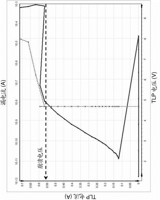
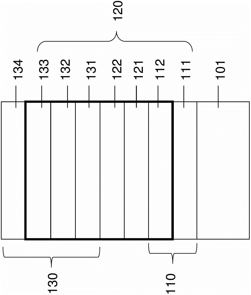
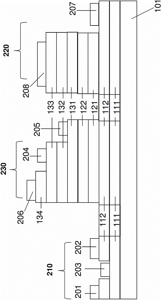
[0024] The compound semiconductor wafer structure integrating the epitaxial structure of a field effect transistor (FET), a heterojunction bipolar transistor (HBT) and a thyristor transistor (Thyristor) provided by the present invention, such as figure 1 As shown, it includes a substrate 101, a field effect transistor epitaxial structure 110, an n-type doped etch stop layer 121, a p-type insertion layer 122 and a heterojunction bipolar transistor structure 130, wherein the substrate 101 The constituent materials can be semi-insulating semiconductor materials such as gallium arsenide (GaAs) or indium phosphide (InP), among which gallium arsenide (GaAs) is preferred; the field effect transistor epitaxial structure 110 is located on the substrate 101 above, including a channel layer 111 and an n-type doped layer 112, wherein the n-type doped layer is located on the channel layer, this structure can be used to make n-type field effect transistors; the n-type doped etch stop layer 1...


PUM


Abstract

The invention relates to a compound semiconductor wafer structure. The compound semiconductor wafer structure comprises a substrate, an n-type field effect transistor expitaxy structure, an n-type adulteration erosion stopping layer, a p-type inserting layer and an npn heterojunction bipolar transistor expitaxy structure, and can be used for manufacturing a field effect transistor or a heterojunction bipolar transistor or a thyristor.

Description

technical field [0001] The present invention relates to a compound semiconductor wafer structure, in particular to a method of integrating a heterojunction bipolar transistor (heterojunction bipolar transistor; HBT), a field effect transistor (field effect transistor; FET) and a gate current transistor (Thyristor) epitaxial structure A single wafer, a compound semiconductor wafer structure that can be applied to an Electrostatic Discharge (ESD) system. Background technique [0002] When the human body touches the integrated circuit, the static electricity accumulated on the human body will enter the circuit through the pins of the integrated circuit, and then discharge through the ground of the integrated circuit. The discharge process will generate a few amperes in just a few hundred nanoseconds (ns). Current may cause abnormal function or damage of integrated circuit components. Therefore, it is usually necessary to design an electrostatic protection system in integrated c...

Claims


Application Information

Patent Timeline
Patent Type & Authority Patents(China)
IPC IPC(8): H01L27/02H01L27/06
Inventor 林正国李思儒许荣豪蔡绪孝
Owner WIN SEMICON
Why Eureka
Try Eureka