Compound semiconductor wafer structure
A semiconductor and compound technology, applied in the field of compound semiconductor wafer structure, can solve the problems of low diode conduction voltage, limited electrostatic protection capability, large wafer area, etc., and achieve low energy consumption, best processing capacity, and reduced use area Effect
- Summary
- Abstract
- Description
- Claims
- Application Information
AI Technical Summary
Problems solved by technology
Method used
Image
Examples
Embodiment Construction
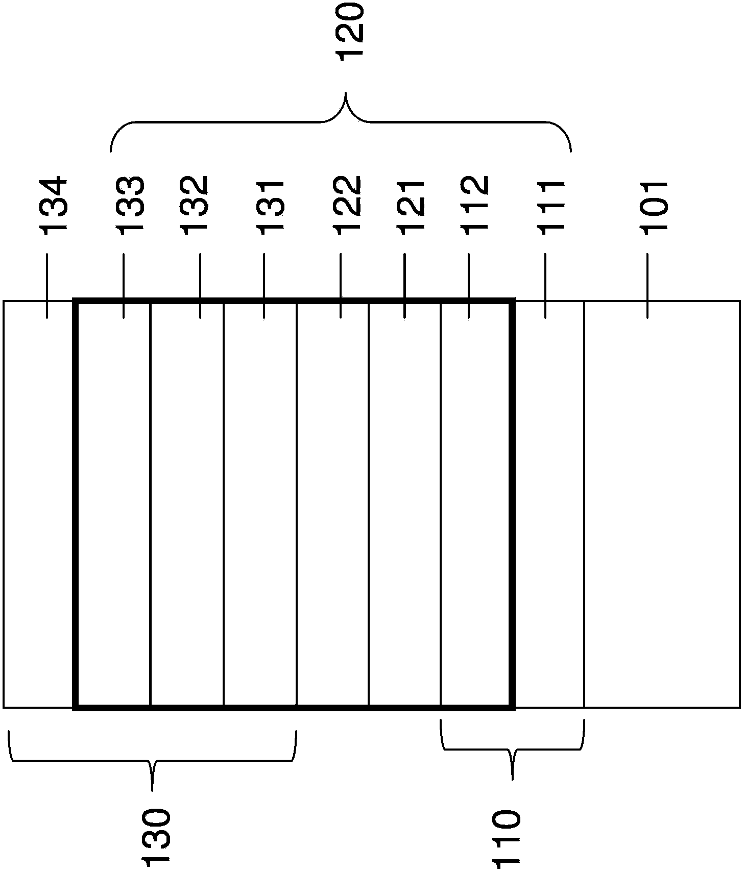
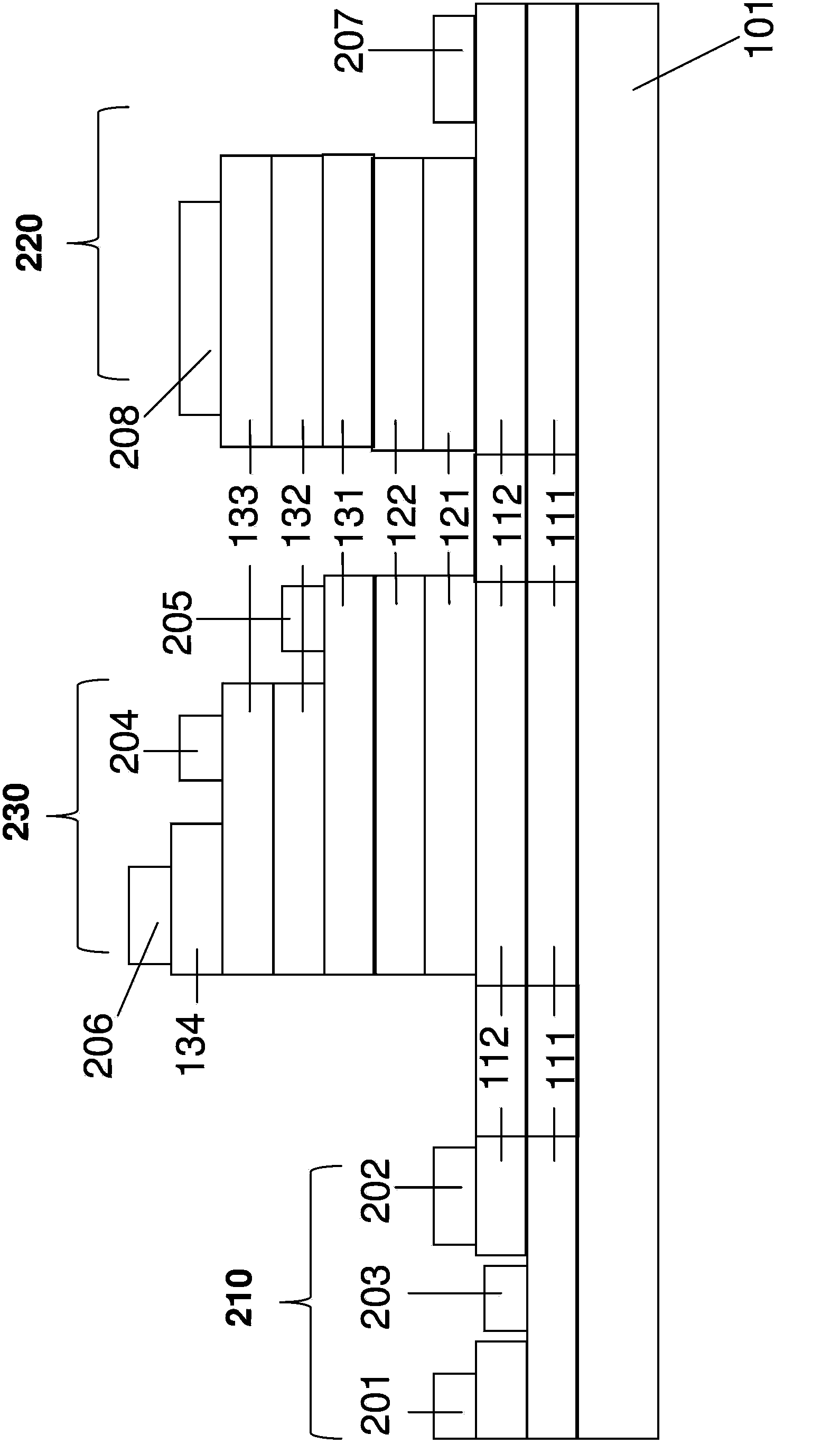
[0024] The compound semiconductor wafer structure integrating the epitaxial structure of a field effect transistor (FET), a heterojunction bipolar transistor (HBT) and a thyristor transistor (Thyristor) provided by the present invention, such as figure 1 As shown, it includes a substrate 101, a field effect transistor epitaxial structure 110, an n-type doped etch stop layer 121, a p-type insertion layer 122 and a heterojunction bipolar transistor structure 130, wherein the substrate 101 The constituent materials can be semi-insulating semiconductor materials such as gallium arsenide (GaAs) or indium phosphide (InP), among which gallium arsenide (GaAs) is preferred; the field effect transistor epitaxial structure 110 is located on the substrate 101 above, including a channel layer 111 and an n-type doped layer 112, wherein the n-type doped layer is located on the channel layer, this structure can be used to make n-type field effect transistors; the n-type doped etch stop layer 1...
PUM
 Abstract
Description
Claims
Application Information


