High-current triggered electrostatic discharge protector

A technology of electrostatic discharge protection and electrostatic discharge, which is applied in the direction of circuits, electrical components, electric solid devices, etc., can solve the problems of crashing and burning semiconductor chips, and achieve the effect of small area

Inactive Publication Date: 2007-03-07
WINBOND ELECTRONICS CORP
View PDF2 Cites 0 Cited by
  • Summary
  • Abstract
  • Description
  • Claims
  • Application Information

AI Technical Summary

Problems solved by technology

If the original voltage on the I / O port before the EMC / ESD test is close to the power supply voltage (~3V), then after the EMC / ESD test, the SCR will maintain the voltage on the I / O port at the holding voltage Vh (~1.6 volts), which will cause a crash on the entire system, and even burn out part of the semiconductor chip

Method used


Image

  • High-current triggered electrostatic discharge protector
  • High-current triggered electrostatic discharge protector
  • High-current triggered electrostatic discharge protector

Examples


Embodiment Construction

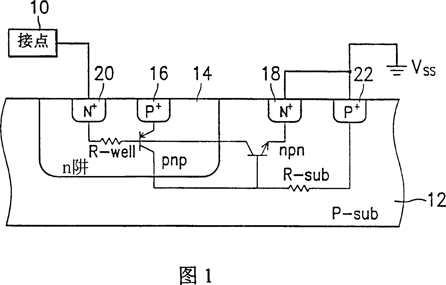
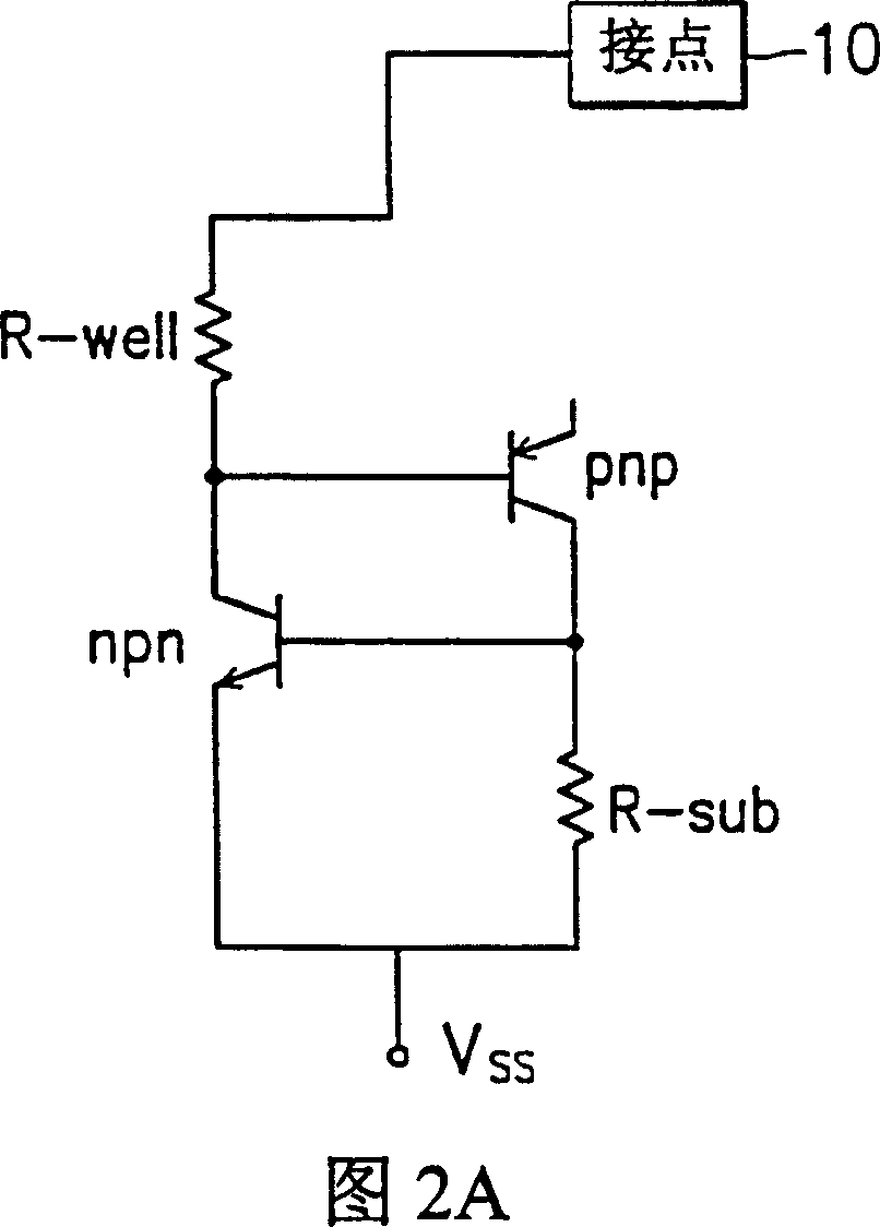
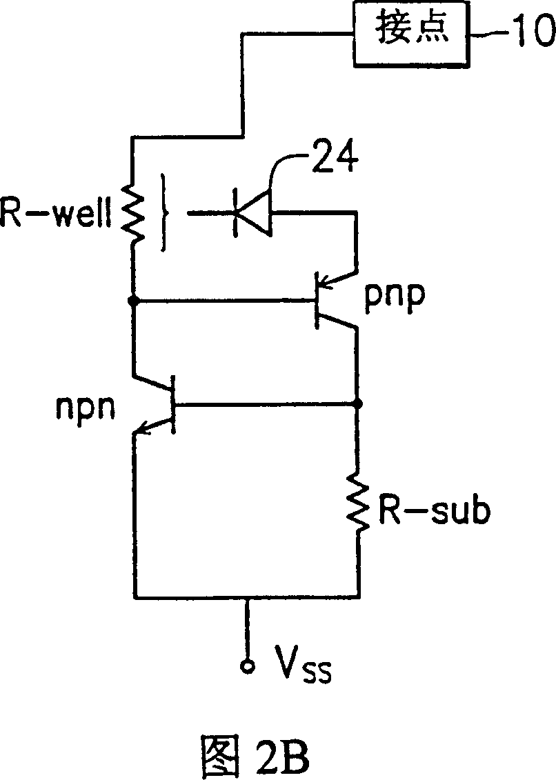
[0038]Please refer to FIG. 1 . FIG. 1 is a schematic cross-sectional view of a first embodiment of the ESD protection circuit of the present invention. The present invention provides an ESD protection circuit for releasing the ESD current on the contact 10 to a reference potential, such as VSS in FIG. 1 . The ESD protection circuit includes a substrate 12 of a first conductivity type, a well region 14 of a second conductivity type, a first doped region 16 of a first conductivity type, a second doped region 18 of a second conductivity type, and a A third doped region 20 of the second conductivity type and a fourth doped region 22 of the first conductivity type. For the convenience of explanation, the first conductivity type is p-type, and the second conductivity type is n-type. The substrate 12 is electrically coupled to the reference potential VSS through the fourth doped region 22 . That is, the fourth doped region 22 is disposed on the surface of the substrate 12 as an ohm...


PUM


Abstract

An electrostatic discharging protection circuit with a high current trigger electrically couples with a contact and a reference potential for discharging the electrostatic discharging current generated from the contact. The electro-static discharging protection circuit contains a first conductive base, a second conductive trap region, a first doped region of the first conduction and a second doped region of the second conduction in which the base couples to the reference potential and the trap region is set at the base coupling to the contact. An electric floating of the first doped region is set at the surface of the trap region. The second doped region is set at the base and coupled to the reference potential. The ESD current of the contact provides a voltage enabling the interface between the trap and the base collasp to trigger a side double-pole transistor made up of the trap region.

Description

technical field [0001] The invention relates to an electrostatic discharge (ESD) protection circuit, especially an ESD protection circuit triggered by high current. The ESD protection circuit of the invention can provide good protection against electrostatic discharge on the one hand, and can avoid ESD on the other hand. The protective circuit latches up during normal operation. Background technique [0002] Generally speaking, in order to protect the finished semiconductor chip from being damaged by the high voltage generated by external static-charged objects, an ESD protection circuit is provided between the input and output ports and the power port of the current semiconductor chip. According to the requirements on the circuit, the ESD protection circuit should be in an open state during normal operation, so that the power port and the input and output ports can maintain normal operation; only when an ESD event occurs at one end of the ESD protection circuit, the ESD pro...

Claims


Application Information

Patent Timeline
Patent Type & Authority Patents(China)
IPC IPC(8): H01L23/60H01L27/00
Inventor 陈伟梵
Owner WINBOND ELECTRONICS CORP
Why Eureka
Try Eureka