Terahertz tuning device based on graphene
A technology of graphene and graphene layers, which is applied in the field of terahertz tuning devices, can solve the problems of small tuning depth and single tuning frequency, and achieve the effect of excellent modulation depth
- Summary
- Abstract
- Description
- Claims
- Application Information
AI Technical Summary
Problems solved by technology
Method used
Image
Examples
specific Embodiment approach 1
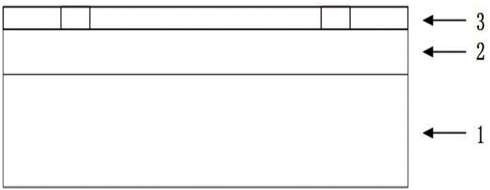
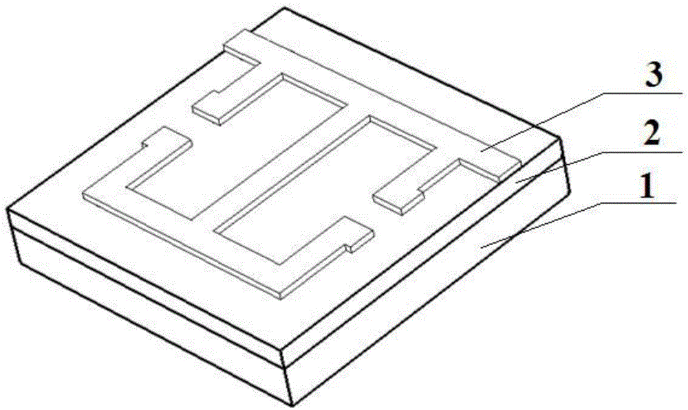
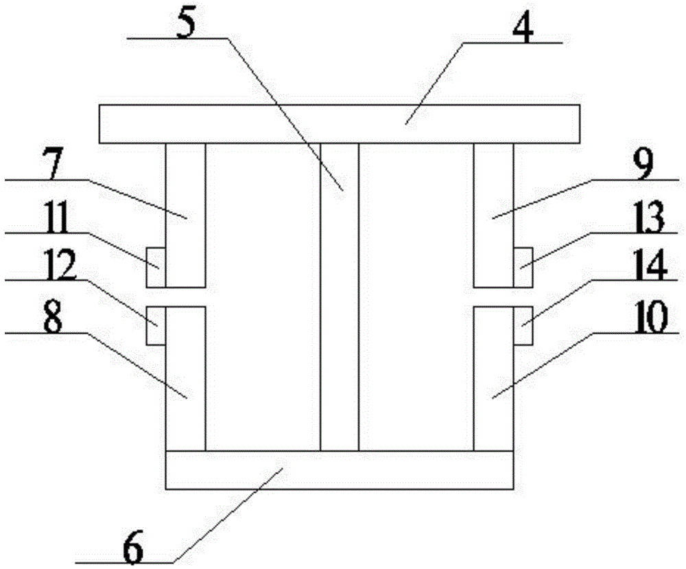
[0011] Specific implementation mode one: as figure 1 , figure 2 and image 3 As shown, a graphene-based terahertz tuning device in this embodiment is composed of a substrate 1, an insulating dielectric layer 2 and a graphene layer 3 with a split resonant ring structure, the substrate 1 is horizontally arranged at the bottom layer, and the The insulating medium layer 2 is arranged in parallel on the upper surface of the substrate 1, and the split resonant ring structure graphene layer 3 is arranged in parallel in the middle of the upper surface of the insulating medium layer 2; the split resonant ring structure graphene layer 3 The shape of the upper surface and the lower surface is the same, the thickness of the split resonator ring structure graphene layer 3 is 0.34 μm, and the upper surface of the split resonator ring structure graphene layer 3 is composed of upper side 4, middle column 5, lower side 6, first The opening edge 7, the second opening edge 8, the third openin...
specific Embodiment approach 2
[0014] Embodiment 2: This embodiment differs from Embodiment 1 in that: the substrate 1 is a square high-resistance silicon plate with a thickness of 500 μm, and its side length is 50 μm; the resistivity of the square high-resistance silicon plate is greater than 10000, the dielectric constant is 11.9. Other steps and parameters are the same as in the first embodiment.
specific Embodiment approach 3
[0015] Embodiment 3: The difference between this embodiment and Embodiment 1 or 2 is that the insulating dielectric layer 2 is a square silicon dioxide plate with a thickness of 3 μm, and its side length is 50 μm; The dielectric constant is 2.88. Other steps and parameters are the same as those in Embodiment 1 or 2.
[0016] In this embodiment, the loss tangent of the square silicon dioxide plate is tan(δ)=0.05, where δ is the loss angle of the insulating medium 2 .
PUM
| Property | Measurement | Unit |
|---|---|---|
| Thickness | aaaaa | aaaaa |
| Thickness | aaaaa | aaaaa |
| Side length | aaaaa | aaaaa |
Abstract
Description
Claims
Application Information


