Supercharge Your Innovation With Domain-Expert AI Agents!

High-energy ion implanter, beam collimator, and beam collimation method

一种射束平行化器、离子注入装置的技术,应用在放电管、电气元件、电路等方向

Active Publication Date: 2015-08-12
SENCORP
View PDF11 Cites 2 Cited by
  • Summary
  • Abstract
  • Description
  • Claims
  • Application Information

AI Technical Summary

Problems solved by technology

[0013] However, in the production of high-quality imaging elements, not only angular accuracy is required, but also many strict requirements such as no metal contamination, small implant damage (residual crystal defects after annealing), good implant depth accuracy (energy accuracy), etc. There are still many things to be improved in the single-wafer ion implantation device

Method used


Image

  • High-energy ion implanter, beam collimator, and beam collimation method
  • High-energy ion implanter, beam collimator, and beam collimation method
  • High-energy ion implanter, beam collimator, and beam collimation method

Examples


Embodiment Construction

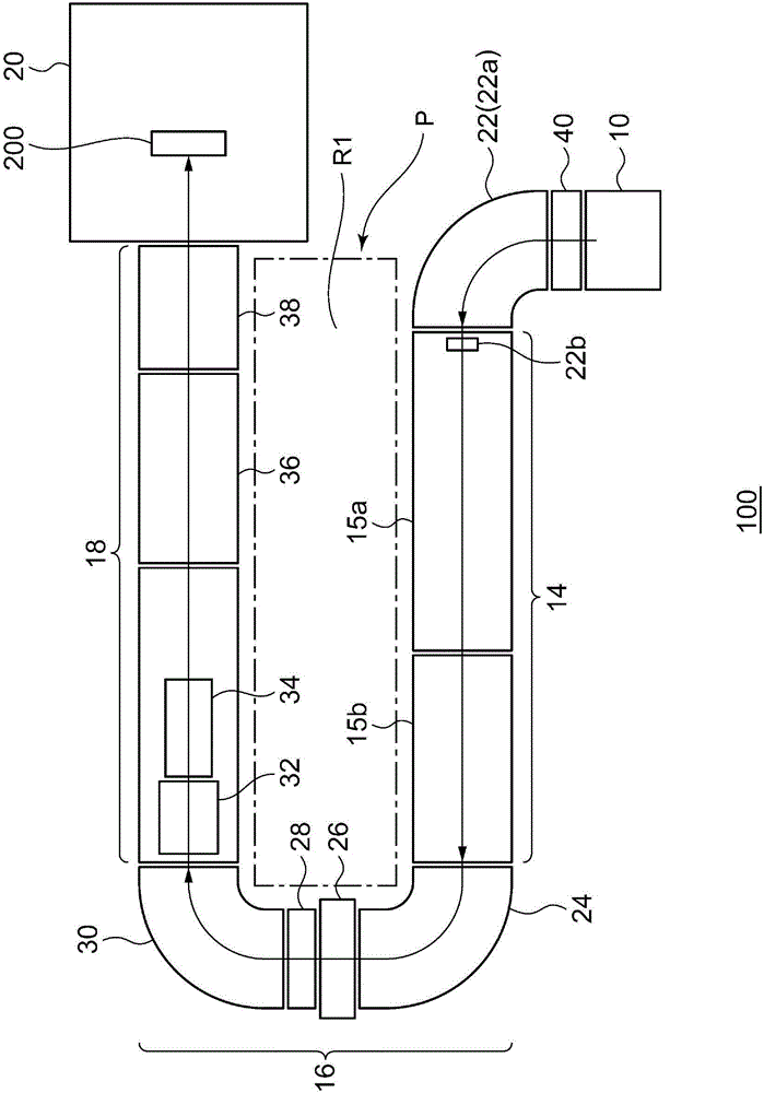
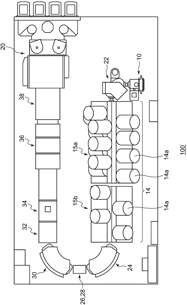
[0059] An example of the high-energy ion implantation apparatus according to this embodiment will be described in more detail below. First, the process by which the present inventors conceived the present invention will be described.

[0060] (parallel magnet)

[0061] A conventional high-energy ion implanter using a parallelizing magnet for parallelizing tracks by a deflection magnetic field has the following problems.

[0062] If high-energy ions are implanted into a wafer with a photoresist layer, a large amount of air leakage will occur, and the molecules of the air leakage will interact with beam ions, and the valence numbers of some ions will change. When the valence changes when passing through the parallelizing magnet, the deflection angle changes, so the parallelism of the beam is broken, and the injection angle toward the wafer becomes different.

[0063] In addition, the amount (number or dose) of implanted ions is obtained by measuring the beam current value with...


PUM


Abstract

A beam collimator includes a plurality of lens units that are arranged along a reference trajectory so that a beam collimated to the reference trajectory comes out from an exit of the beam collimator. Each of the plurality of lens units forms a bow-shaped curved gap and is formed such that an angle of a beam traveling direction with respect to the reference trajectory is changed by an electric field generated in the bow-shaped curved gap. A vacant space is provided between one lens unit of the plurality of lens units and a lens unit that is adjacent to the lens unit. The vacant space is directed in a transverse direction of the collimated beam in a cross section that is perpendicular to the reference trajectory. An inner field containing the reference trajectory is connected to an outer field of the plurality of lens units through the vacant space.

Description

technical field [0001] This application claims priority based on Japanese Patent Application No. 2014-023531 filed on February 10, 2014. The entire content of this application is incorporated in this specification by reference. [0002] The invention relates to a high-energy ion implantation device. Background technique [0003] In the manufacturing process of semiconductor elements, an important process for adding impurities to the crystal of the semiconductor wafer by implanting ions into the semiconductor wafer under vacuum to change the conductivity and make the semiconductor Wafer semiconductor components. The device used in this process is called an ion implantation device, and the ion implantation device accelerates impurity atoms as ions and implants them into the semiconductor wafer. [0004] With the high integration and high performance of semiconductor elements, devices capable of performing high-energy ion implantation to penetrate deeper into semiconductor w...

Claims


Application Information

Patent Timeline
Patent Type & Authority Applications(China)
IPC IPC(8): H01J37/317H01J37/08
CPCH01J37/3171H01J2237/31701H01J37/15H01J37/1472H01J2237/152H01J37/3007H01J37/10H01J2237/103H01J37/08H01J37/317H01J37/12H01J2237/024H01J2237/032H01J2237/121H01J2237/16H01J37/147
Inventor 加藤浩二天野吉隆
Owner SENCORP
Features
  • R&D
  • Intellectual Property
  • Life Sciences
  • Materials
  • Tech Scout
  • Unparalleled Data Quality
  • Higher Quality Content
  • 60% Fewer Hallucinations
Learn More