Chip packaging method and chip packaging structure

A chip packaging and chip technology, applied in the field of chip packaging method and chip packaging structure, can solve the problems of packaging quality and packaging structure integration degree to be improved, and achieve the effect of avoiding the problem of alignment deviation, simple forming process and stable combination.

Inactive Publication Date: 2015-08-12
CHINA WAFER LEVEL CSP
View PDF6 Cites 19 Cited by
  • Summary
  • Abstract
  • Description
  • Claims
  • Application Information

AI Technical Summary

Problems solved by technology

[0004] However, the packaging quality of the existing fan-out wafer level packaging method and the integration level of the formed packaging structure still need to be improved

Method used


Image

  • Chip packaging method and chip packaging structure
  • Chip packaging method and chip packaging structure
  • Chip packaging method and chip packaging structure

Examples


Embodiment Construction

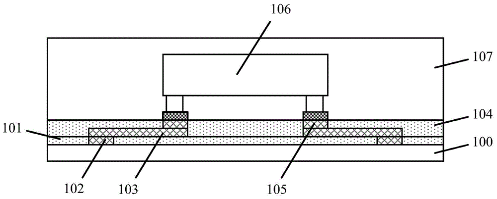
[0042] As mentioned in the background, the packaging quality of the existing fan-out wafer level packaging method and the integration degree of the formed packaging structure still need to be improved.

[0043] Please refer to figure 1 , figure 1 It is an embodiment of a fan-out wafer level packaging structure, including: a carrier 100; a release film and a first dielectric layer 101 located on the surface of the carrier 100; a first opening located in the first dielectric layer 101; a first opening located in the first dielectric layer 101; The substrate end metal electrode 102 in the opening; the wiring layer 103 located on the surface of the first dielectric layer 101; the second dielectric layer 104 located on the surface of the wiring layer 103, the substrate end metal electrode 102 and the first dielectric layer 101, the There is a second opening in the second dielectric layer 104; the chip-side metal electrode 105 positioned in the second opening; the functional surfac...


PUM


Abstract

The invention provides a chip packaging method and a chip packaging structure, wherein the chip packaging method comprises the steps of providing a first chip which comprises a first surface and a second surface that oppose each other, wherein the first surface of the first chip is provided with a plurality of first pads; providing a second chip with a third surface and a fourth surface that oppose each other, wherein the third surface of the second chip is provided with a plurality of second pads and the area of the second chip is larger than that of the first chip; providing a carrier plate; combining the fourth surface of the second chip with the surface of the carrier plate, wherein the plurality of second pads are arranged outside the combining area between the first chip and the second chip; forming a sealing material layer on the surface of the carrier plate, wherein the sealing material layer packages the first chip and the second chip; and forming a first conductive structure and a second conductive structure in the sealing material layer, wherein the first conductive structure is electrically connected with the first pads and the second conductive structure is electrically connected with the second pads. A package which is formed according to the chip packaging method has advantages of reduced structural dimension, improved stability and improved reliability.

Description

technical field [0001] The invention relates to the technical field of semiconductor manufacturing, in particular to a chip packaging method and a chip packaging structure. Background technique [0002] Wafer Level Chip Size Packaging (WLCSP) technology is a technology in which a wafer is packaged and tested and then cut to obtain a single finished chip. The size of the packaged chip is exactly the same as that of the bare chip. Wafer-level chip-scale packaging technology has completely subverted traditional packaging, such as ceramic leadless chip carrier (Ceramic Leadless Chip Carrier) and organic leadless chip carrier (Organic Leadless Chip Carrier), etc. , small, short, thin and low-cost requirements. The size of the chip packaged by the wafer-level chip size packaging technology can be highly miniaturized, and the cost of the chip is significantly reduced with the reduction of the chip size and the increase of the wafer size. Wafer-level chip-scale packaging technolog...

Claims


Application Information

Patent Timeline
Patent Type & Authority Applications(China)
IPC IPC(8): H01L25/04H01L23/488H01L23/29
CPCH01L23/29H01L24/07H01L24/81H01L25/074H01L23/488H01L2224/32145H01L2924/15174H01L2224/24146H01L24/19H01L24/20H01L24/24H01L24/82H01L2224/04105H01L2224/12105H01L2224/24195H01L2224/32225H01L2224/73267H01L2224/82005H01L2224/92244H01L2224/97H01L2924/18162H01L2224/8203H01L21/568H01L2224/16227H01L2224/24145H01L2924/15313H01L2924/19105H01L24/97H01L2224/83H01L2224/19H01L2224/83005H01L2224/16225H01L2224/18H01L24/01H01L2224/24153H01L2224/32227
Inventor 王之奇杨莹王蔚
Owner CHINA WAFER LEVEL CSP
Why Eureka
Try Eureka