

Electrochemical polishing device and method
A polishing device and electrochemical technology, applied in the field of integrated circuit manufacturing, can solve the problems of different removal rate and polishing uniformity, and achieve the effect of compact structure and improved processing efficiency
- Summary
- Abstract
- Description
- Claims
- Application Information
AI Technical Summary
Problems solved by technology
Method used
Image

Examples
Embodiment Construction
[0024] In order to describe the technical content, structural features, achieved goals and effects of the present invention in detail, the following will be described in detail in conjunction with the embodiments and accompanying drawings.
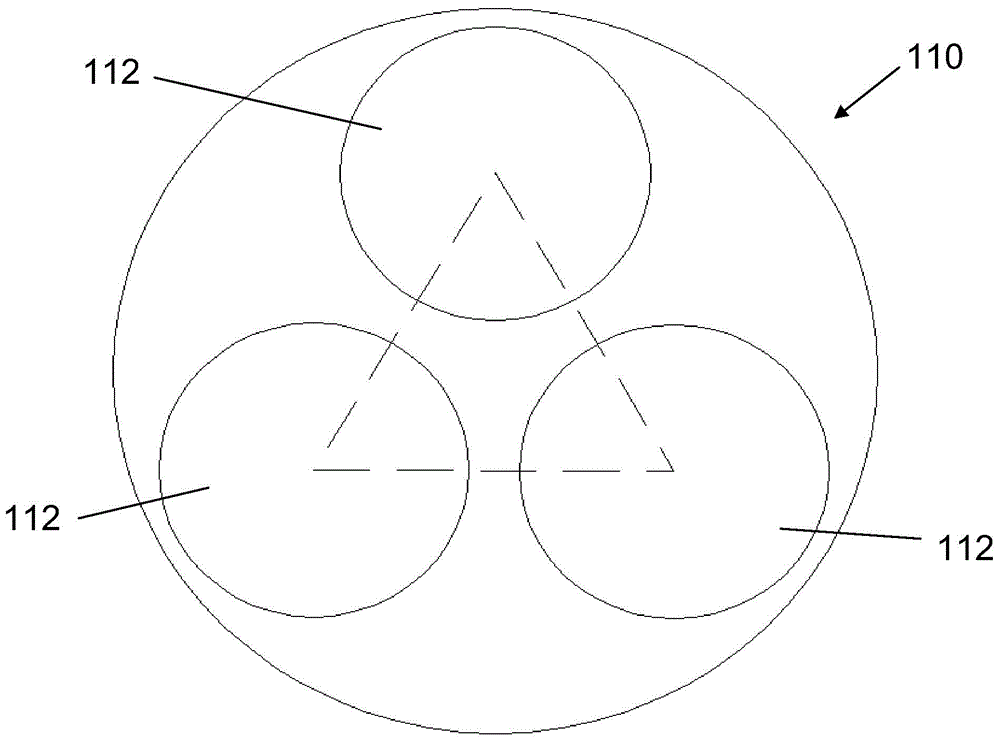
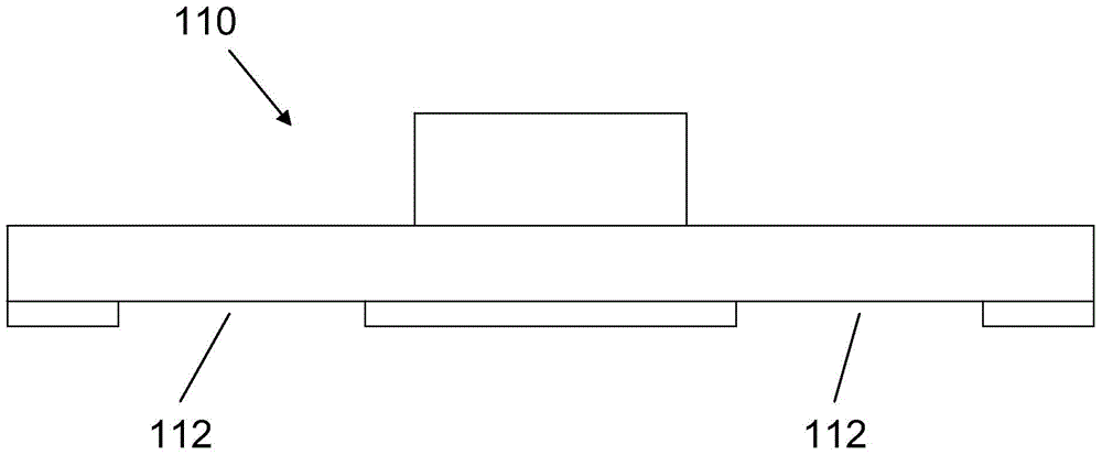
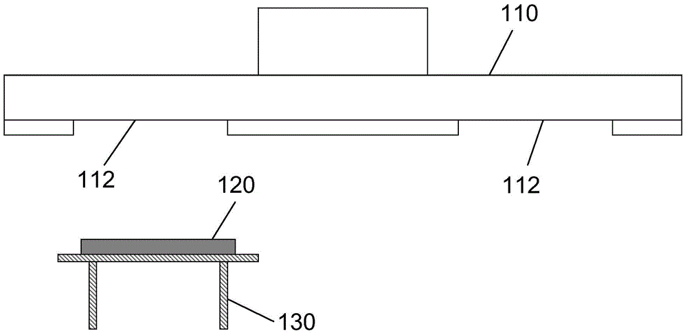
[0025] refer to figure 1 and figure 2 , which discloses a bottom view and a schematic cross-sectional structure diagram of a wafer chuck of an electrochemical polishing device according to an embodiment of the present invention. In one embodiment, the wafer chuck 110 suitable for electrolytic polishing is provided with several wafer grooves 112, and the several wafer grooves 112 are evenly distributed from the center of the wafer chuck 110 to the outside of the wafer chuck 110 between the edges. The diameters of the several wafer grooves 112 are equal, and the centers of the several wafer grooves 112 are distributed on concentric circles centered on the center of the wafer chuck 110 . In the illustrated embodiment, the three wafer groo...
PUM
 Abstract
Description
Claims
Application Information