Method for forming Y-shaped gate metal dielectric hole through auxiliary of photoresist

An auxiliary medium and photoresist technology, applied in electrical components, circuits, semiconductor devices, etc., can solve the problems of small size and reduced gate parasitic capacitance, and achieve a reduction in gate parasitic capacitance and significant reduction in gate parasitic capacitance. Effect

Active Publication Date: 2015-08-26
NO 55 INST CHINA ELECTRONIC SCI & TECHNOLOGYGROUP CO LTD
View PDF7 Cites 0 Cited by
  • Summary
  • Abstract
  • Description
  • Claims
  • Application Information

AI Technical Summary

Problems solved by technology

The traditional gate dielectric void formation method utilizes the dielectric deposition gas to have different mass transport rates at different positions under the gate metal, resulting in different growth rates to form plugged voids. As shown in Figure 1, the dielectric voids obtained by this method are usually The size is small, so the reduction of gate parasitic capacitance is limited

Method used


Image

  • Method for forming Y-shaped gate metal dielectric hole through auxiliary of photoresist
  • Method for forming Y-shaped gate metal dielectric hole through auxiliary of photoresist
  • Method for forming Y-shaped gate metal dielectric hole through auxiliary of photoresist

Examples


Embodiment Construction

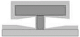
[0037] The method for forming a Y-shaped gate metal dielectric cavity assisted by photoresist includes the following five steps:

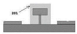
[0038] 1) After gate metallization, apply photoresist, carry out pattern photolithography and development, and form as shown in Figure 2-a, Figure 2-b The auxiliary photoresist pattern shown forms a cover 201 for the gate metal strip.

[0039] 2) Low temperature growth of SiN medium 200nm, as shown in Figure 3-a, Figure 3-b As shown; the growth temperature of the medium should be low (using ICP-PECVD, 60°C), otherwise the photoresist will be deformed or even flow due to heat; the thickness of the medium should not be too small, otherwise it will be easily broken in the subsequent decoating process.

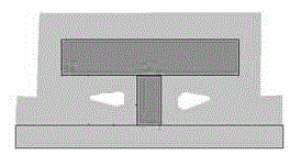
[0040] 3) Photolithography forms photoresist mask patterns (for dielectric etching) (401, 402) as shown in Figure 4-a and 4-b; perform SiN dielectric etching, after dielectric etching, the lower layer assists The photoresist is exposed at both end...


PUM


Abstract

The invention provides a method for forming a Y-shaped gate metal dielectric hole through auxiliary of photoresist. The method comprises the following steps that 1) coverage of photoresist on a Y-shaped gate metal strip is formed through the photoetching technology; 2) SiN dielectric is grown at low temperature; 3) dielectric holing is performed at the two end heads of the gate metal strip through the photoetching and dielectric etching technology; 4) a Y-shaped gate dielectric hole is formed by removing photoresist of a sacrificial layer; and 5) the grown SiN dielectric seals the dielectric holes of the two end heads of the gate metal strip. Advantages are that the gate metal dielectric hole formed by the method is larger and reduction of gate parasitic capacitance is more significant so that the method has positive significance in reducing device gate parasitic capacitance of submicron and deep submicron gate length second-generation and third-generation semiconductor field effect devices of millimeter wave applications.

Description

technical field [0001] The invention relates to a method for improving the high-frequency performance and noise performance of second-generation and third-generation semiconductor field-effect devices with submicron and deep submicron gate lengths, which relies on photoresist to assist in forming a Y-shaped gate metal dielectric cavity. It belongs to the field of semiconductor technology. Background technique [0002] For microwave and millimeter wave field effect transistors, one of the main means to improve their frequency characteristics is to reduce the gate length of the device to reduce the channel electron transit time; the development of small gate length GaAs and InP HMET / PHEMT devices at home and abroad has reached less than 100nm level. For such a small gate length, the greatly increased gate resistance has become an important factor restricting device performance; in order to solve the problem of large gate resistance of devices with small gate lengths, T-shaped...

Claims


Application Information

Patent Timeline
Patent Type & Authority Applications(China)
IPC IPC(8): H01L21/28
CPCH01L29/401H01L29/42364
Inventor 韩克锋
Owner NO 55 INST CHINA ELECTRONIC SCI & TECHNOLOGYGROUP CO LTD
Why Eureka
Try Eureka