A kind of gan HEMT device and preparation method

A device and gate dielectric layer technology, applied in semiconductor/solid-state device manufacturing, semiconductor devices, electrical components, etc., can solve problems such as fluctuations, parasitic parameter changes, and affecting device frequency characteristics, so as to achieve simple operation, improve device frequency characteristics, The effect of reducing process difficulty and cost

Active Publication Date: 2020-09-01
河北中瓷电子科技股份有限公司石家庄高新区分公司
View PDF5 Cites 0 Cited by
  • Summary
  • Abstract
  • Description
  • Claims
  • Application Information

AI Technical Summary

Problems solved by technology

[0003] The purpose of the embodiments of the present invention is to provide a GaN HEMT device and its preparation method, aiming to solve the problem that when the distance between the source electrode and the drain electrode of the GaN HEMT device is reduced, fluctuations in the gate overlay process lead to changes in parasitic parameters, thereby affecting the frequency characteristics of the device. , which uses the double-groove structure gate groove prepared in the gate dielectric layer to avoid parasitic parameter changes caused by gate overlay process fluctuations, thereby reducing process difficulty and improving process stability and device frequency characteristics

Method used


Image

  • A kind of gan HEMT device and preparation method
  • A kind of gan HEMT device and preparation method
  • A kind of gan HEMT device and preparation method

Examples


Embodiment 1

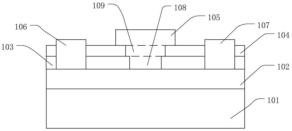
[0045] The GaN HEMT device in this embodiment includes a substrate, and the upper surface of the substrate is sequentially provided with a GaN epitaxial layer and a gate dielectric layer from bottom to top, and also includes a gate, a source electrode and a drain electrode; the gate, The source electrode and the drain electrode penetrate through the gate dielectric layer and are in contact with the GaN epitaxial layer; the gate dielectric layer includes a first gate dielectric layer and a second gate dielectric layer with different properties; A first gate groove that runs through the first gate dielectric layer, and a second gate groove that penetrates the second gate dielectric layer is opened on the second gate dielectric layer; wherein, the positions of the first gate groove and the second gate groove are Corresponding; the gate includes gate metal filling the first gate groove and the second gate groove, and a gate cap arranged on the upper surface of the second dielectric...

Embodiment 2

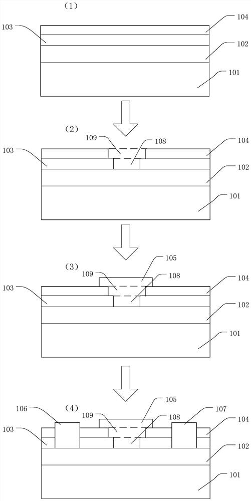
[0051] see figure 2 (1), figure 2 It is a cross-sectional view of the process structure of the preparation method of the GaN HEMT device. The GaN HEMT device includes a substrate 101 , a GaN epitaxial layer 102 , a first gate dielectric layer 103 and a second gate dielectric layer 104 .

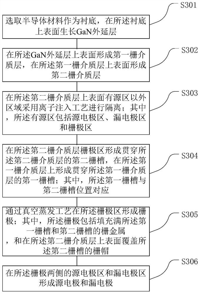
[0052] see image 3 , this embodiment discloses a method for fabricating a GaN HEMT device, which is described in detail as follows:

[0053] In step S301, a semiconductor material is selected as a substrate, and a GaN epitaxial layer is grown on the upper surface of the substrate.

[0054] Optionally, SiC, Si, etc. can be used as the substrate.

[0055] Step S302, forming a first gate dielectric layer on the upper surface of the GaN epitaxial layer, and forming a second gate dielectric layer on the upper surface of the first gate dielectric layer.

[0056] Optionally, the specific implementation method of step S302 is: preparing a first gate dielectric with a thickness of 100nm-200nm ...


PUM

PropertyMeasurementUnit
thicknessaaaaaaaaaa
thicknessaaaaaaaaaa
lengthaaaaaaaaaa

Abstract

The invention relates to the technical field of semiconductor devices, and discloses a GaN HEMT device and a preparation method thereof, including a substrate, a GaN epitaxial layer and a gate dielectric layer are sequentially arranged on the upper surface of the substrate from bottom to top, and a GaN epitaxial layer and a GaN epitaxial layer are also included. The grid, the source electrode and the drain electrode in layer contact; the gate dielectric layer includes a first gate dielectric layer and a second gate dielectric layer with different properties; a first gate groove is opened on the first gate dielectric layer, and a first gate groove is opened on the second gate dielectric layer A second gate groove is opened, and the position of the first gate groove corresponds to the position of the second gate groove; the gate includes gate metal filling the first gate groove and the second gate groove, and a gate cap arranged on the upper surface of the second dielectric layer; Source and drain electrodes are located on both sides of the gate. The present invention can effectively reduce gate parasitic capacitance and improve device frequency characteristics by providing gate grooves with steep sidewalls and double-groove structures at the corresponding positions of two gate dielectric layers with different properties.

Description

technical field [0001] The invention relates to the technical field of semiconductor devices, in particular to a GaN HEMT device and a preparation method. Background technique [0002] At present, GaN HEMT (High Electron Mobility Transistor) devices have excellent power and frequency characteristics, high breakdown and low noise characteristics, and are widely used in mobile communications, radar and other fields. In order to improve the frequency characteristics of GaN HEMT devices, it is not only necessary to shorten the length of the gate, but also to reduce the parasitic parameters of the device, such as: parasitic capacitance, parasitic inductance, parasitic resistance, etc. Reducing the square resistance of the material and shortening the distance between the source electrode and the drain electrode are the main ways to reduce the parasitic resistance. When the distance between the source electrode and the drain electrode is reduced, the overlay of the gate becomes th...

Claims


Application Information

Patent Timeline
Patent Type & Authority Patents(China)
IPC IPC(8): H01L29/778H01L21/335
CPCH01L29/66462H01L29/7787H01L29/7788H01L29/2003H01L29/42316H01L29/778
Inventor 张力江高渊高昶王国清宋洁晶付兴昌
Owner 河北中瓷电子科技股份有限公司石家庄高新区分公司
Why Eureka
Try Eureka