Trench type power semiconductor device and manufacturing method thereof

A power semiconductor, trench-type technology, applied in semiconductor/solid-state device manufacturing, semiconductor devices, electrical components, etc., can solve problems such as high process risk, increase the difficulty and cost of device manufacturing, short circuit between gate and emitter, and achieve Reduce manufacturing costs, speed up switching, and avoid the effects of parasitic gate capacitance

Active Publication Date: 2020-09-29
安建科技(深圳)有限公司
View PDF8 Cites 2 Cited by
  • Summary
  • Abstract
  • Description
  • Claims
  • Application Information

AI Technical Summary

Problems solved by technology

However, in order to reduce the gate parasitic capacitance introduced by the trench (105) to accelerate the switching speed of the device, the surface area of ​​the trench (105) needs to be reduced, which leads to the narrower width of the trench (105) generally being set (about 1 μm), and in the process of device processing, there is often a certain alignment deviation in the contact hole photolithography process. If the contact hole on the gate trench deviates slightly, it will easily cause the gap between the gate and the emitter. Short circuit, the process risk is too high, and the use of high-precision photolithography alignment process will increase the difficulty and cost of device manufacturing, resulting in more losses than gains

Method used


Image

  • Trench type power semiconductor device and manufacturing method thereof
  • Trench type power semiconductor device and manufacturing method thereof
  • Trench type power semiconductor device and manufacturing method thereof

Examples


Embodiment 1

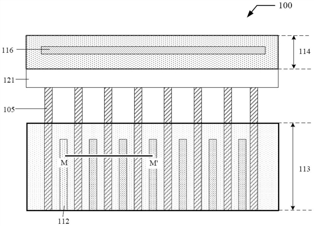
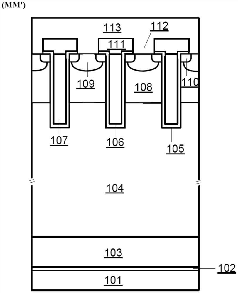
[0057] image 3 It is a schematic partial top view of the IGBT device 200 based on the first embodiment of the present invention, Figure 4 and Figure 5 corresponding to image 3 A schematic diagram of the cross-sectional structure of the A-A' and B-B' tangent lines of the middle device 200. Such as Figure 4 , 5 As shown, the device 200 has a collector metal layer (201) at the bottom of the device, a semiconductor region above the collector metal layer (201), and the semiconductor region includes p + type collector doped region (202), n type electric field stop layer (203) and n - type drift region (204); an interlayer dielectric layer (211) is provided on the semiconductor region, and the interlayer dielectric layer is generally made of materials such as silicon oxide or silicon nitride; in the interlayer dielectric layer ( 211) are respectively provided with an emitter electrode metal layer (213) and a gate electrode metal layer (214) composed of metal layers, such a...

Embodiment 2

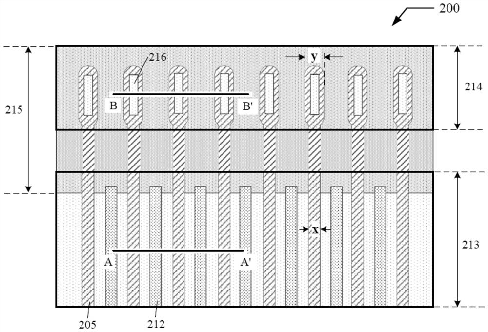
[0063] Figure 24 is a schematic partial top view of an IGBT device 300 according to a second embodiment of the present invention, Figure 25 and Figure 26 corresponding to Figure 24 The schematic diagram of the cross-sectional structure of the C-C' and D-D' tangent lines of the middle device 300. Compared with the device 200 described above, the device 300 also has the following characteristics: there are several dummy trenches (218) arranged in parallel with the trenches (205), and the start of the dummy trenches (218) Both the initial section and the extension section are located under the emitter electrode metal layer (213), and the width of the initial section of the dummy trench (218) is greater than the width of its extension section. The dummy trench (218) is filled with a dummy gate conductive material (227), and a dummy gate contact hole (217) is provided above the initial section of the dummy trench (218), and the dummy gate conductive material (227) is connec...

Embodiment 3

[0065] Figure 27 is a schematic partial top view of an IGBT device 400 according to a third embodiment of the present invention, Figure 28 and Figure 29 corresponding to Figure 27 Schematic diagram of the cross-sectional structure of the E-E' and F-F' tangent lines of the middle device 400. Compared with the device 300 described above, the device 400 also has the following characteristics: there is more than one dummy trench (218) between adjacent trenches (205), and the dummy trenches (218) between adjacent dummy trenches (218) No emitter contact hole (212) is provided on the surface of the semiconductor region. A p-type body region (208) may be provided between the extensions of adjacent dummy trenches (218), such as Figure 28 shown. Since there is no emitter contact hole (212) between adjacent dummy trenches (218), the semiconductor region in this region can be in an electrically floating state, so more carriers can be stored when the IGBT is in the on-state, Red...


PUM

PropertyMeasurementUnit
widthaaaaaaaaaa
widthaaaaaaaaaa

Abstract

The invention discloses a trench type power semiconductor device and a manufacturing method thereof, and relates to a power semiconductor device. In order to solve the problems that the manufacturingcost of a device is increased and the parasitic gate capacitance is increased due to the presence of a gate bus, the invention provides the following technical scheme: a gate contact hole is formed inan interlayer dielectric layer above the initial section of a trench, the gate conductive material in the trench is connected with the gate electrode metal layer above the gate conductive material through the gate contact hole, the width of the gate contact hole is smaller than that of the initial section of the trench, and the width of the initial section of the trench is larger than that of theextension section of the trench. The beneficial effects of the invention are that: according to the trench type power semiconductor device, stable and reliable grid connection can be realized on thebasis of not causing negative influence on the performance of the device; and by omitting a gate bus board, the photoetching process steps of the device are reduced, and the manufacturing cost of thedevice is reduced; and meanwhile, the gate parasitic capacitance introduced by the gate bus board is reduced, and the switching speed of the device is improved.

Description

technical field [0001] The invention relates to the structural design and manufacturing method of power semiconductor devices, especially trench power transistors, such as insulated gate bipolar transistors (IGBT) and power metal oxide semiconductor field effect transistors (Power MOSFET). Background technique [0002] Power transistors are a key component of power electronics systems and are widely used in various applications such as motor drives and power conversion. Generally, power transistors mainly include Power Metal Oxide Semiconductor Field Effect Transistors (Power MOSFETs), Insulated Gate Bipolar Transistors (IGBTs), etc. The former is mainly suitable for medium and low voltage (≤600V) low power systems, and the latter is mainly suitable for Medium and high voltage high power (≥600V) high power system. From the perspective of the structure of power transistors, there are mainly two structures, planar gate and trench gate. Among them, the trench gate structure ca...

Claims


Application Information

Patent Timeline
Patent Type & Authority Applications(China)
IPC IPC(8): H01L29/739H01L29/423H01L21/331
CPCH01L29/7397H01L29/4236H01L29/66348
Inventor 单建安冯浩
Owner 安建科技(深圳)有限公司
Why Eureka
Try Eureka