Optical module receiver and 1*9 optical module

A technology of optical modules and receivers, which is applied in the field of optical communication, can solve problems such as low stability, complicated debugging, and unsatisfactory requirements, and achieve the effects of stable performance, low circuit cost, and simple debugging methods

Inactive Publication Date: 2015-08-26
成都新易盛通信技术股份有限公司
View PDF8 Cites 4 Cited by
  • Summary
  • Abstract
  • Description
  • Claims
  • Application Information

AI Technical Summary

Problems solved by technology

Most of the receivers of these modules use PIN (PIN photodiode) devices, so the transmission distance is mostly within 100km. When longer distance transmission is required, it basically cannot meet the requirements.
[0007] To sum up, the bias voltage compensation circuit in the prior art has high cost, low stability, and complicated debugging. At the same time, the existing 1×9 optical module is difficult to achieve long-distance transmission.

Method used


Image

  • Optical module receiver and 1*9 optical module
  • Optical module receiver and 1*9 optical module
  • Optical module receiver and 1*9 optical module

Examples


Embodiment Construction

[0023] The present invention will be further described in detail below in conjunction with specific embodiments. However, it should not be understood that the scope of the above-mentioned subject of the present invention is limited to the following embodiments, and all technologies implemented based on the content of the present invention belong to the scope of the present invention.

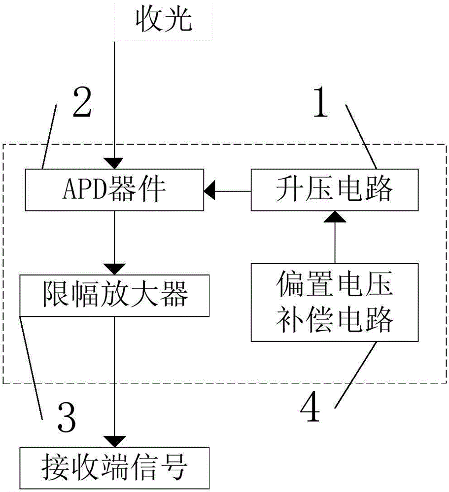
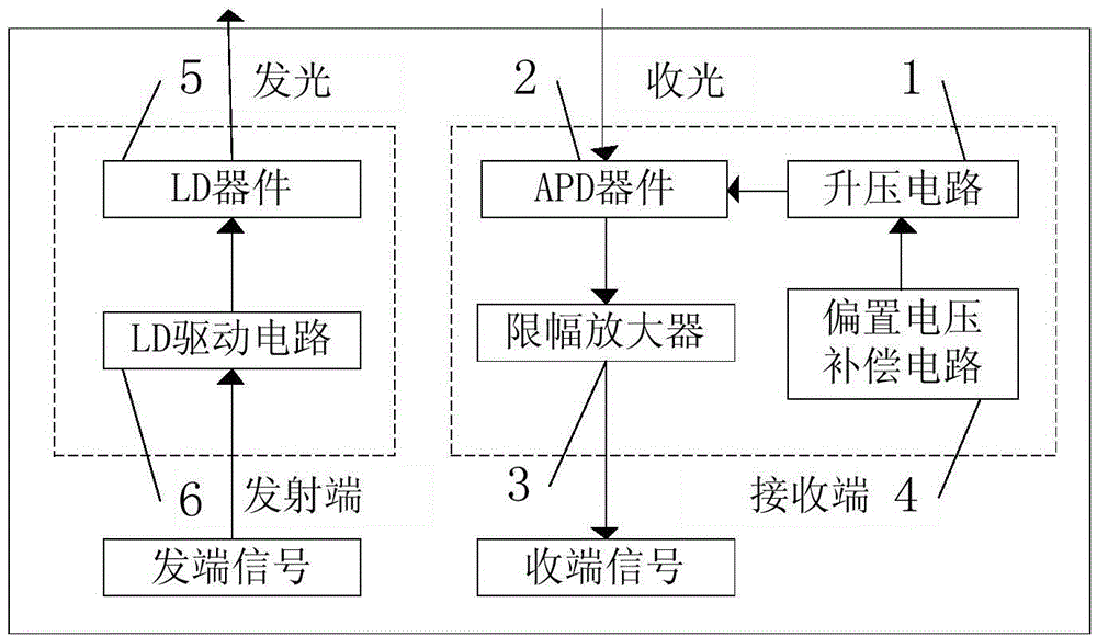
[0024] figure 1 It is an optical module receiving end of the present invention, including a boost circuit 1, a limiting amplifier 3, and an APD device 2. The boost circuit 1 is connected to the APD device 2, and the APD device 2 is connected to the limiting amplifier 3. It also includes a bias voltage compensation circuit 4.

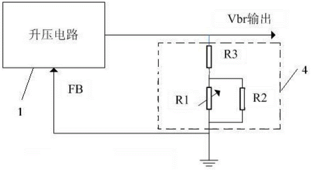
[0025] The bias voltage compensation circuit uses a thermal element to control the boost circuit for adjusting the voltage value output by the boost circuit when the temperature of the APD element changes to make the APD element work in an avalanche state .

[0026] Compared wi...


PUM


Abstract

The invention discloses an optical module receiver, comprising a boosted circuit, a limiting amplifier, and an avalanche photo diode (APD) device. The boosted circuit is connected with the APD device. The APD device is connected with the limiting amplifier. The optical module receiver is characterized by also comprising a bias voltage compensating circuit. The bias voltage compensating circuit is connected with the boosted circuit. The bias voltage compensating circuit uses a thermosensitive element to control the boosted circuit and is used for adjusting the voltage value output by the boosted circuit when the temperature of the APD element changes. The optical module receiver has low cost, stable performance, and a simple method. The invention also discloses a 1*9 optical module, comprising an optical module transmitter and also comprising the optical module receiver disclosed by the invention. The 1*9 optical module can support long distance (greater than 100KM) transmission.

Description

Technical field [0001] The present invention relates to the field of optical communication, in particular to an optical module receiver and a 1×9 optical module. Background technique [0002] APD (Avalanche Photo Diode avalanche photodiode) is a PN junction type photodetection diode, which uses the avalanche multiplication effect of carriers to amplify the photoelectric signal to improve the sensitivity of detection, which provides for long-distance (more than 100KM) transmission Condition. [0003] APD needs to add a larger reverse bias voltage Vbr when working to make it achieve the avalanche multiplier effect. 1×9 optical modules generally supply power for 3.3V or 5V, which cannot meet the higher voltage required by APD devices, so a boost circuit is required. In addition, as the characteristics of the APD device change with temperature, the corresponding Vbr will also change. In order to maintain high sensitivity, when the temperature changes, a bias voltage compensation cir...

Claims


Application Information

Patent Timeline
Patent Type & Authority Applications(China)
IPC IPC(8): H04B10/40H04B10/60
Inventor 高伟明宛明刘宇然倪晓龙邢鑫尹磊
Owner 成都新易盛通信技术股份有限公司
Why Eureka
Try Eureka