Method for optimizing wafer exposure sequences

An optimization method and wafer technology, applied in the direction of microlithography exposure equipment, photolithography exposure equipment, etc., can solve the problems of reducing output, achieve the effect of improving product yield, avoiding lens thermal effect, and reducing movement

Active Publication Date: 2015-09-09
SHANGHAI HUALI MICROELECTRONICS CORP
View PDF5 Cites 3 Cited by
  • Summary
  • Abstract
  • Description
  • Claims
  • Application Information

AI Technical Summary

Problems solved by technology

But the downside of this approach is that if the lens heating conditions are acceptable, add

Method used


Image

  • Method for optimizing wafer exposure sequences
  • Method for optimizing wafer exposure sequences
  • Method for optimizing wafer exposure sequences

Examples


Embodiment Construction

[0026] In order to make the objectives, technical solutions and advantages of the present invention clearer, the embodiments of the present invention will be further described in detail below with reference to the accompanying drawings. Those skilled in the art can easily understand other advantages and functions of the present invention from the content disclosed in this specification. The present invention can also be implemented or applied through other different specific embodiments, and various details in this specification can also be modified or changed based on different viewpoints and applications without departing from the spirit of the present invention.

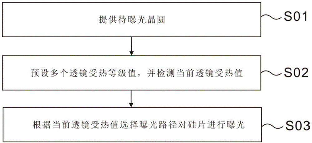
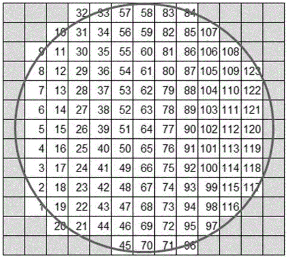
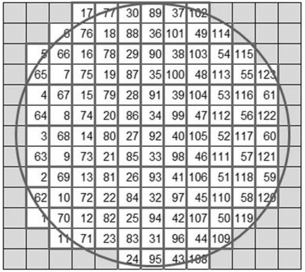
[0027] The above and other technical features and beneficial effects will be combined with the embodiments and appendix Figures 1 to 4 The method for optimizing the wafer exposure sequence of the present invention will be described in detail. figure 1 It is a schematic flowchart of the method for optimizing the ...


PUM


Abstract

The invention discloses a method for optimizing wafer exposure sequences. The method comprises the following steps: firstly, providing a to-be-exposed wafer; presetting a plurality of lens heating level values; detecting the current lens heating level value; and finally selecting an exposure path to expose the silicon wafer according to the current lens heating level value. According to the method for optimizing the wafer exposure sequences disclosed by the invention, different exposure sequences are selected according to the lens heating values; the movement of a slide holder is reduced; the lens heat effect is avoided; meanwhile, improvement of the capacity is taken into account; by virtue of the method for optimizing the wafer exposure sequence disclosed by the invention, a relatively good process alignment precision can be obtained; and the yield of a product is improved.

Description

technical field [0001] The invention belongs to the field of semiconductor integrated circuit manufacturing equipment, and relates to a method for optimizing the exposure sequence of wafers. Background technique [0002] With the rapid development of semiconductor technology and the continuous improvement of the integration level of integrated chips, the manufacturing process of the chips is becoming more and more complicated. In order to ensure a higher yield, the requirements for the entire process flow and equipment will be more stringent. The basic principle of lithography is to use the characteristics of photoresist (or photoresist) to form corrosion resistance due to photochemical reaction after exposure to engrave the pattern on the mask onto the surface of the wafer to be processed. superior. In the exposure process, since the size of the exposure area of ​​the exposure system at one time is limited, it is necessary to divide a wafer into a plurality of exposure uni...

Claims


Application Information

Patent Timeline
IPC IPC(8): G03F7/20
Inventor 王晓龙陈力钧李德建朱骏
Owner SHANGHAI HUALI MICROELECTRONICS CORP
Why Eureka
Try Eureka