Unlock instant, AI-driven research and patent intelligence for your innovation.

Array substrate and making method thereof, display panel, and display device

A technology of an array substrate and a manufacturing method, which is applied in the field of display devices, and can solve problems such as the influence of leakage current of thin film transistors, sensitivity to light irradiation, and influence on the quality of display images

Inactive Publication Date: 2015-09-09
BOE TECH GRP CO LTD +1
View PDF9 Cites 10 Cited by
  • Summary
  • Abstract
  • Description
  • Claims
  • Application Information

AI Technical Summary

Problems solved by technology

However, the active layer 11 of the thin film transistor is more sensitive to the irradiation of light
like figure 1 As shown, when the light from the side indicated by the arrow (such as ambient light) irradiates the active layer 11, the leakage current of the thin film transistor will be affected, thereby causing crosstalk, voltage flicker and other phenomena, and then affecting the display screen. quality

Method used


Image

  • Array substrate and making method thereof, display panel, and display device
  • Array substrate and making method thereof, display panel, and display device
  • Array substrate and making method thereof, display panel, and display device

Examples


Embodiment Construction

[0029] Specific embodiments of the present invention will be described in detail below in conjunction with the accompanying drawings. It should be understood that the specific embodiments described here are only used to illustrate and explain the present invention, and are not intended to limit the present invention.

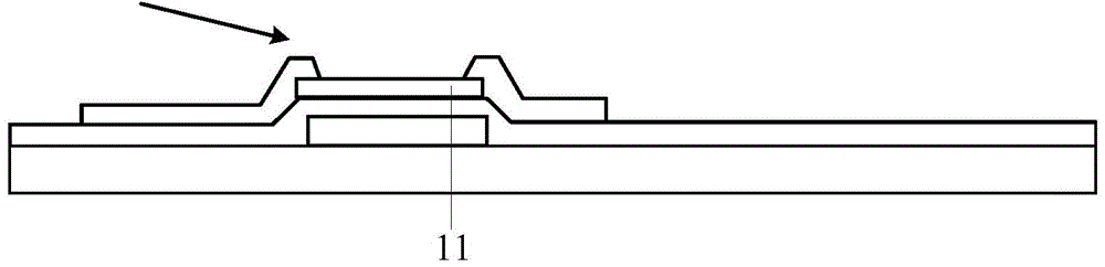
[0030] As a first aspect of the present invention, an array substrate is provided, such as figure 2 As shown, it includes a substrate 10 and a thin film transistor disposed on the substrate, the thin film transistor includes an active layer 11, and the array substrate further includes a light shielding layer 12 disposed above the active layer of the thin film transistor, The light shielding layer 12 at least covers the channel region of the thin film transistor.

[0031] In the present invention, since the light-shielding layer 12 covers at least the channel region of the thin film transistor, it can reduce the side light entering the channel region of the thi...


PUM


Abstract

The invention discloses an array substrate and a making method thereof, a display panel, and a display device. The array substrate includes a substrate and a thin film transistor arranged on the substrate. The thin film transistor includes an active layer. The array substrate further includes a shading layer which is arranged above the active layer of the thin film transistor, and the shading layer at least covers a channel region of the thin film transistor. Illumination of light on the active layer is reduced, leakage current is reduced, the occurrence of crosstalk, voltage flicker, residual image and other phenomena is reduced, and the display effect is improved.

Description

technical field [0001] The present invention relates to the field of display technology, in particular to an array substrate, a display panel including the array substrate, and a display device including the display panel. Background technique [0002] The liquid crystal panel includes an array substrate and a cell substrate. The array substrate is provided with gate lines and data lines. The gate lines and data lines define a plurality of pixel units. Each pixel unit is provided with a thin film transistor. The gate of the thin film transistor is connected to the Corresponding gate lines are connected, and when the voltage on the gate lines reaches the turn-on voltage, the source and drain of the thin film transistors are turned on, so that the data voltage on the data lines is input to the pixel electrodes. However, the active layer 11 of the TFT is relatively sensitive to light irradiation. Such as figure 1 As shown, when the light from the side indicated by the arrow (...

Claims


Application Information

Patent Timeline
IPC IPC(8): H01L27/12H01L21/77
Inventor 李晓光刘晓伟
Owner BOE TECH GRP CO LTD