A detection structure and detection method of a photomask

A detection method and photomask technology, applied in the semiconductor field, can solve the problems of not being detected, the risk of detection results, etc.

Active Publication Date: 2019-12-17
SEMICON MFG INT (SHANGHAI) CORP
View PDF5 Cites 0 Cited by
  • Summary
  • Abstract
  • Description
  • Claims
  • Application Information

AI Technical Summary

Problems solved by technology

[0005] After completing the preparation of the PSM, it is necessary to detect the defects of the PSM to get rid of the defects in the PSM. In the inspection of the defects, it is not necessary to detect the chromium grains, so the chromium crystals Set the chromium grains as the do not inspect region (do not inspection region, DNIR), set other regions as inspection regions, and detect the PSM. At present, there are three methods for setting the chromium grains as DNIR, as follows: Figure 1a-1c as shown in Figure 1a As shown, an inspection area 11 is set in the chromium grain 10, the area of ​​the inspection area is smaller than the area of ​​the chromium grain 10, so as to exclude the chromium grain from the detection area, but the The problem with the method is that there is still a large part between the chromium grain 10 and the inspection area that has not been detected, such as Figure 1a As shown in the area 12 filled in the upper left corner of the center, it brings great risks to the detection results; the second method is as follows Figure 1b As shown, firstly, the inspection area 11 is set on the inner side of the array of chromium grains 10, so that the outermost frame of the chromium grains 10 is set as DNIR, and then a cutting line is set in the array of chromium grains Array, the scribe line array is a plurality of horizontal or vertical strip structures, so as to cover the horizontal and vertical frames inside the chromium grain array to form a DNIR area, but the disadvantage of the method is that it cannot Set the oblique frame inside the chromium grain array as the DNIR area; the third method is as attached Figure 1c As shown, wherein the method is a further improvement to the second method, specifically increasing the width of the vertically arranged dicing lines so as to cover the hypotenuse of the chromium grains to form a DNIR region, But the shortcoming of described method is, described kerf coverage area is too big, causes such as Figure 1c The area 12 filled in the upper left corner of the center cannot be detected, and there are similar areas in each chromium grain, which brings great risk to the detection results

Method used


Image

  • A detection structure and detection method of a photomask
  • A detection structure and detection method of a photomask
  • A detection structure and detection method of a photomask

Examples


Embodiment 1

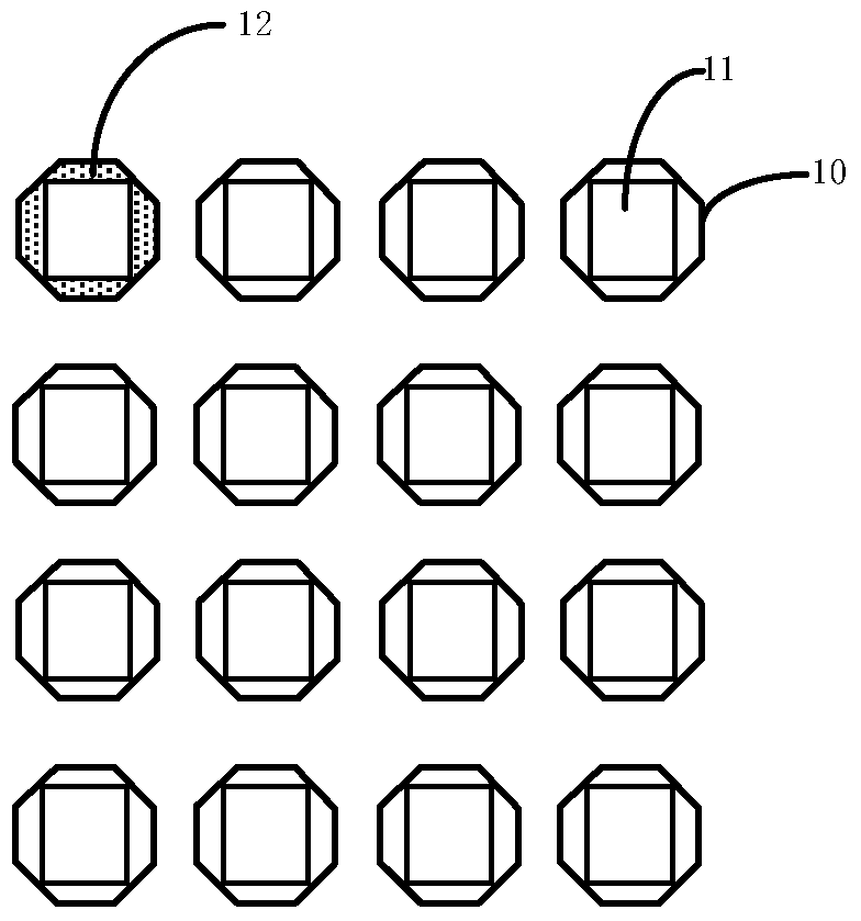
[0054] The detection method of the photomask of the present invention will be further described below in conjunction with the accompanying drawings. In this embodiment, the phase shift photomask is used as an example for illustration, but it should be noted that this embodiment is only for illustrative purposes. The above method is not limited to the phase shift mask, and can also be applied to a type of mask in which the chromium grain pattern is set as a non-detection area.

[0055] The method of the present invention comprises:

[0056] Step (a) providing a phase shift mask, the phase shift has a chromium grain array composed of mutually isolated chromium grains 20;

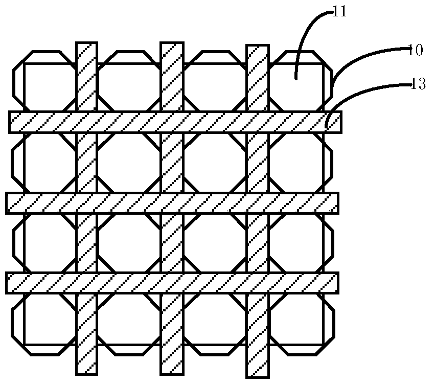
[0057] Step (b) Determine the scope of the inspection area 21 in the phase shift mask, so that the outermost horizontal frame and vertical frame in the chromium grain array are set outside the inspection area 21, set to non- inspection area;

[0058] Step (c) setting a first non-inspection area array 22 in t...

Embodiment 2

[0084] The present invention also provides a detection structure of a phase shift mask, including:

[0085] A chromium grain array, located in the phase shift mask, including chromium grains 20 isolated from each other;

[0086] The inspection area 21 is located in the phase shift mask, so that the outermost horizontal frame and vertical frame in the chromium grain array are set outside the inspection area 21 and set as a non-inspection area;

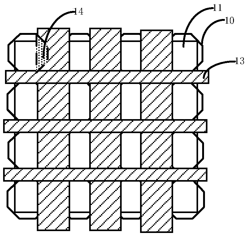
[0087] The first non-inspection area array 22 is located in the phase shift mask covering the horizontal frame and the vertical frame of the chromium grains inside the chromium grain array to form a non-inspection area;

[0088] The second non-inspection area array 23 is located in the inspection area 21 and covers the hypotenuse frame inside the chromium grain array to form a non-inspection area.

[0089]Wherein, the detection structure further includes a third non-inspection area array 24 , which is located in the phase shift mask an...


PUM


Abstract

The invention relates to a photomask detection structure and a detection method thereof. The method comprises the following steps: a)providing a photomask, wherein the photomask has a chromium crystal rings array composed of mutual-isolated chromium crystal rings; b)determining a scope of an inspection area in the photomask, arranging a horizontal frame and a vertical frame at most external side in the chromium crystal ring array in the inspection area, setting as a non-inspection area; c)setting a first non-inspection area array in the photomask, covering the horizontal frame and the vertical frame in the chromium crystal ring array to form the non-inspection areal; d)arranging a second non-inspection area array in the photomask, covering a beveling frame of the chromium crystal ring in the chromium crystal ring array to form the non-inspection area. The method can ensure the largest detection area and the smallest which can be obtained, defect existence risk is reduced, and the obtained accurate detection result is more accurate.

Description

technical field [0001] The invention relates to the field of semiconductors, and in particular, the invention relates to a detection structure and a detection method of a photomask. Background technique [0002] With the continuous development of semiconductor technology, the preparation of semiconductor devices tends to be miniaturized, and has been developed to the nanometer level, while the preparation process of conventional devices is gradually mature. In the manufacturing process of semiconductor devices, the design circuit is firstly obtained by lithography imaging, and then the design pattern is precisely defined on the photomask through the manufacturing process, and the pattern on the photomask is transferred to the semiconductor substrate by using the etching process to manufacture Get the required line structure. [0003] With the continuous development of semiconductor technology, Phase Shift Mask (PSM) has been widely used. PSM adopts double-exposure (Double-e...

Claims


Application Information

Patent Timeline
Patent Type & Authority Patents(China)
IPC IPC(8): G03F1/44
CPCG03F1/44
Inventor 凌文君
Owner SEMICON MFG INT (SHANGHAI) CORP
Why Eureka
Try Eureka