Thin film packaging device
A thin-film packaging and device technology, which is applied in the direction of electric solid-state devices, semiconductor devices, organic semiconductor devices, etc., can solve the problems affecting the structural stability of the isolation layer and device functional layer, and the inability to use desiccant in thin-film packaging.
- Summary
- Abstract
- Description
- Claims
- Application Information
AI Technical Summary
Problems solved by technology
Method used
Image
Examples
Embodiment 1
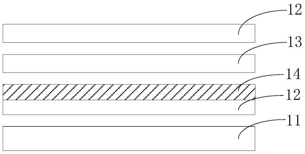
[0037] Please refer to image 3 , the thin film encapsulation device includes a substrate 11 , a barrier layer 12 , a functional layer 13 and a drying layer 14 . Wherein, the functional layer 13 includes a first surface and a second surface opposite to the first surface; the barrier layer 12 is arranged on the first surface and the second surface of the functional layer 13, and at least one barrier layer 12 At least a part or all of it is a dry layer 14, and the dry layer 14 includes a substrate 141 and a groove-shaped grid 142, the groove-shaped grid 142 is arranged on the surface of the substrate 141, and the groove-shaped grid 142 is filled with desiccant. The substrate 141 may be a structure similar to the barrier layer 12 or a structure supporting the groove-shaped grid 142 .
[0038] In this embodiment, the functional layer 13 is sandwiched by two barrier layers 12 to protect the functional layer 13 from the upper and lower directions, wherein the functional layer 13 c...
Embodiment 2
[0042] Please refer to Figure 7 , which is another preferred embodiment, the thin film encapsulation device is respectively a second barrier layer 21, a functional layer 22, a first dry layer 23, a first barrier layer 24 and a substrate 25 from top to bottom, and the structure can be better To prevent the infiltration of water vapor and oxygen, the double-layer protection can be achieved, and a barrier layer can also be added around the device, which can effectively prevent the infiltration of water vapor and oxygen at the edge. The structure of the first drying layer 23 is also a groove-shaped grid (not shown), the desiccant is filled in the groove-shaped grid, and the desiccant is bound by the groove-shaped grid to increase the binding capacity of the desiccant to achieve a good drying effect. At the same time, it can also prevent the desiccant from detaching without affecting the light transmittance.
[0043] Take the present embodiment as an example below to illustrate t...
Embodiment 3
[0047] Please refer to Figure 7 and Figure 8 , is another thin-film device packaging structure. Based on the second embodiment, the positions of the substrate 25 and the first barrier layer 24 are exchanged. This structure can also protect the device well. In this embodiment, the flexible substrate may also contain a barrier layer.
PUM
 Abstract
Description
Claims
Application Information


