Array substrate, preparation method thereof and display device

A technology of an array substrate and a manufacturing method, which is applied in the field of display, can solve problems such as potential differences, and achieve the effects of slowing down the flow speed, enhancing the blocking effect, and preventing ESD phenomena

Active Publication Date: 2015-09-23
BOE TECH GRP CO LTD
View PDF2 Cites 0 Cited by
  • Summary
  • Abstract
  • Description
  • Claims
  • Application Information

AI Technical Summary

Problems solved by technology

[0004] However, static electricity is easily generated during the process of depositing the second insulating layer 5, and the electrostatic charge will accumulate on the source-drain connection portion 4 below the second insulation layer 5, causing a gap between the source-drain connection portion 4 and the gate connection portion 2. Potential difference
Since the resistance of the bridge portion 6 electrically connecting the gate connection portion 2 and the source-drain connection portion 4 is relatively low, the electrostatic charge flows quickly, resulting in the end of the gate connection portion 2 and the source-drain connection portion 4 being close (as shown in FIG. 1 ). Shown by the dotted circle in ) produces ESD (Electro Static Discharge, electrostatic discharge) phenomenon

Method used


Image

  • Array substrate, preparation method thereof and display device
  • Array substrate, preparation method thereof and display device
  • Array substrate, preparation method thereof and display device

Examples


Embodiment 1

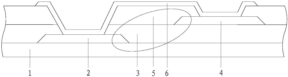
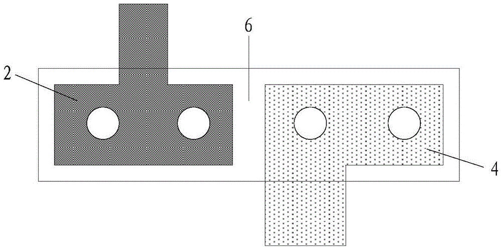
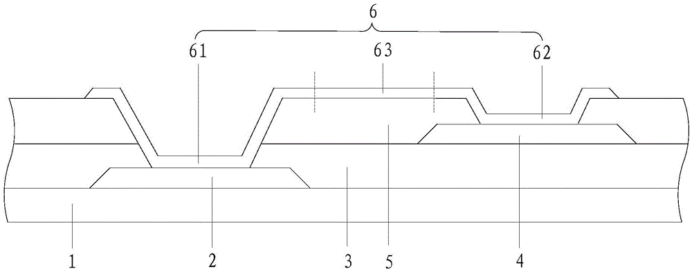
[0048] This embodiment provides an array substrate, such as Figure 2a and 2b As shown, it includes: a base substrate 1 , and a gate electrode layer, a first insulating layer 3 , a source-drain electrode layer, a second insulating layer 5 and a transparent conductive layer stacked on the base substrate 1 in sequence. The gate electrode layer includes a gate connection portion 2 , the source-drain electrode layer includes a source-drain connection portion 4 , and the transparent conductive layer includes a bridging portion 6 .

[0049] Wherein, the bridging portion 6 includes: a first electrode 61 electrically connected to the gate connecting portion 2; a second electrode 62 electrically connected to the source-drain connecting portion 4; a connecting electrode 63, one end of which connecting electrode 63 is electrically connected to the first electrode 61. connected, and the other end is electrically connected to the second electrode 62.

[0050] Taking the surface perpendic...

Embodiment 2

[0066] Based on the technical solution provided by Embodiment 1, in this embodiment, a compensation electrode electrically connected to the bridge portion 6 is provided to enhance the connection between the gate connection portion 2 and the source-drain connection portion 4 after the electrostatic charge in the source-drain connection portion 4 is released. The conductive performance between the parts 4 compensates for the loss of the conductive performance between the gate connection part 2 and the source-drain connection part 4 caused by increasing the resistance of the bridge part 6 .

[0067] Specifically, such as Figure 3a and Figure 3b As shown, the array substrate provided in this embodiment further includes: a third insulating layer 9 covering the transparent conductive layer; a third via hole 11 penetrating through the third insulating layer 9 and located above the first electrode 61; penetrating through the third insulating layer 9 and the fourth via hole 12 locat...

Embodiment 3

[0073] Based on Embodiment 1, in this embodiment, a part of the source-drain electrode layer pattern to be connected in the source-drain electrode layer is used as the source-drain connection part, or a part of the gate electrode layer pattern to be connected in the gate electrode layer is used as the gate connection part, The occupied area of ​​the pattern in the gate electrode layer and the pattern in the source-drain electrode layer that are electrically connected is reduced, and the structure of the array substrate is simplified.

[0074] The scheme of using a part of the pattern of the source-drain electrode layer to be connected as the source-drain connection part can specifically be as follows: Figure 4 As shown, the source-drain electrode layer also includes: a source-drain electrode layer pattern 13 to be connected, the source-drain electrode layer pattern 13 to be connected includes a source, a drain and a data line, and the second via hole 8 is located at the source...


PUM

PropertyMeasurementUnit
Sizeaaaaaaaaaa

Abstract

The invention provides an array substrate, a preparation method thereof and a display device, relates to the technical field of display, and aims at preventing the array substrate from ESD phenomenon in the production process. The array substrate comprises a grid connection portion, a source-drain connection portion and a bridging portion; and the bridging portion comprises a first electrode, a second electrode and a connecting electrode, wherein the first electrode is electrically connected with the grid connection portion, the second electrode is electrically connected with the source-drain connection portion, and the two ends of the connecting electrode are electrically connected with the first and the second electrodes respectively. A surface vertical to a substrate body and successively through the first electrode, the connecting electrode and the second electrode serves as a reference surface, the area of the cross section where the connecting electrode is vertical to both the substrate body and the reference surface is lower than that of the cross section where the first electrode is vertical to both the substrate body and the reference surface, and the area of the cross section where the connecting electrode is vertical to both the substrate body and the reference surface is lower than that of the cross section where the second electrode is vertical to both the substrate body and the reference surface. The array substrate is used to compose the display device.

Description

technical field [0001] The present invention relates to the field of display technology, in particular to an array substrate, a manufacturing method thereof, and a display device. Background technique [0002] The array substrate is an important part of the display device, and the array substrate mainly includes: a base substrate, a gate electrode layer, a first insulating layer, an active layer, a source-drain electrode layer, a second insulating layer and a transparent conductive layer. Wherein, the patterns in the gate electrode layer may include gates and gate lines, the patterns in the source-drain electrode layer may include source electrodes, drain electrodes and data lines, and the patterns in the transparent conductive layer may include pixel electrodes. [0003] In many areas of the array substrate, it is necessary to electrically connect the pattern in the gate electrode layer and the pattern in the source-drain electrode layer, such as: electrically connect diffe...

Claims


Application Information

Patent Timeline
IPC IPC(8): H01L27/12H01L23/60
CPCH01L27/124H01L27/0292H01L27/1248H01L29/41733H01L29/42384H01L27/1222H01L23/535H01L29/786
Inventor 金熙哲
Owner BOE TECH GRP CO LTD
Why Eureka
Try Eureka