Method for preventing punch through voltage between bit lines from decreasing and semiconductor memory

A punch-through voltage and semiconductor technology, applied in the direction of semiconductor devices, semiconductor/solid-state device manufacturing, electric solid-state devices, etc., can solve the problems of reducing the punch-through voltage and not finding it, and achieve the effect of increasing the resistance and avoiding the reduction of the punch-through voltage

Active Publication Date: 2010-06-09
SEMICON MFG INT (SHANGHAI) CORP
View PDF1 Cites 0 Cited by
  • Summary
  • Abstract
  • Description
  • Claims
  • Application Information

AI Technical Summary

Problems solved by technology

However, the inventors of the present application have found in experiments that even if a staggered design is adopted, a leakage current path still occurs near the bit line contact hole 103 (such as image 3 shown by the middle arrow), which greatly reduces the punch-through voltage between adjacent bit lines (V PT ), and the prior art has not discovered the problem and the reason for the problem, and has not given a solution to the problem

Method used


Image

  • Method for preventing punch through voltage between bit lines from decreasing and semiconductor memory
  • Method for preventing punch through voltage between bit lines from decreasing and semiconductor memory
  • Method for preventing punch through voltage between bit lines from decreasing and semiconductor memory

Examples


Embodiment Construction

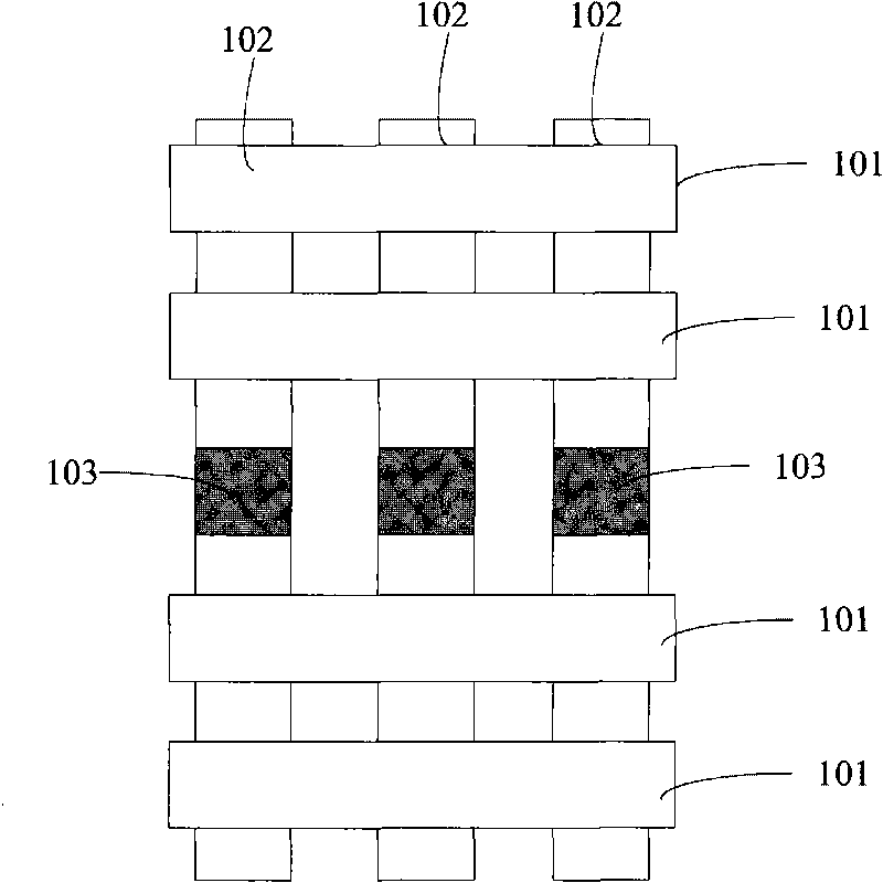
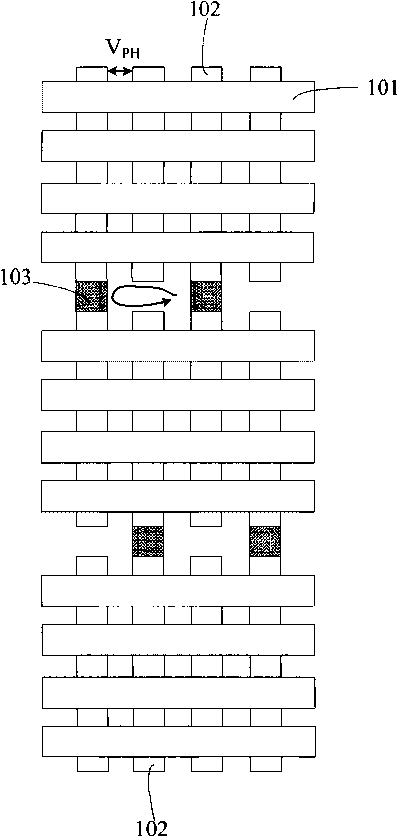
[0032] The present invention increases the doping concentration in the semiconductor substrate of the ion-doped region by forming an ion-doped region opposite to the conductivity type of the source / drain in the region between the closest word lines in the adjacent memory array , and the resistance between the bit lines in the semiconductor substrate is increased, thereby avoiding the defect that leakage current channels appear in the contact hole area of ​​the bit lines in the prior art, thereby reducing the punch-through voltage between adjacent bit lines.

[0033] Below by describing specific embodiment in detail according to accompanying drawing, above-mentioned object and advantage of the present invention will be clearer:

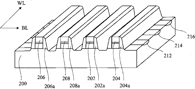
[0034] The present invention firstly provides a method for preventing the drop-through voltage between the bit lines of the memory, referring to Figure 4 , comprising: performing step S11, providing a semiconductor substrate, in which word lines are f...


PUM


Abstract

The invention discloses a method for preventing punch through voltage between bit lines from decreasing and a semiconductor memory. The method for preventing punch through voltage between bit lines from decreasing comprises the steps of providing a semiconductor substrate in which word lines are formed; and forming an ion doping zone in the area between the most proximal word lines in the adjacent memory array, wherein the conductive type of the ion doping zone is opposite to that of the source / drain electrode formed in the semiconductor substrate. By forming the ion doping zone in the area between the most proximal word lines in the adjacent memory array, the invention further increases the doping concentration of the ion doping zone in the semiconductor substrate and enhances the resistance between the bit lines in the semiconductor substrate, thus avoiding the defect that the punch through voltage between bit lines decreases in the prior art.

Description

technical field [0001] The invention relates to the technical field of semiconductors, in particular to a method for preventing drop-through voltage between bit lines of a memory and a semiconductor memory. Background technique [0002] Semiconductor memory is a semiconductor device used to store data or data. In the storage of data data, the capacity of the memory is represented by bits (Bit). Each unit used to store data is called a storage unit (Cell). The storage units are arranged in an array in the memory, and each combination of row and column represents a specific storage unit address. Wherein, multiple memory cells in the same row or column are connected in series through a common wire. Wherein, the wires connecting memory cells in the same row (or the same column) in series are called word lines, and the wires related to data transmission are called bit lines. [0003] figure 1 It is a top view of a memory structure in the prior art, including word lines 101 ,...

Claims


Application Information

Patent Timeline
IPC IPC(8): H01L21/8247H01L27/115
Inventor 王培仁闫锋司伟林竞尧杨帆衣冠君
Owner SEMICON MFG INT (SHANGHAI) CORP
Why Eureka
Try Eureka