Junction termination structure comprising fusion resistor, and manufacturing method thereof
A junction termination and resistance technology, used in semiconductor/solid-state device manufacturing, circuits, electrical components, etc., can solve problems such as electric field concentration at the main junction, and achieve the effects of reducing electric field strength, increasing resistance, and high reliability
- Summary
- Abstract
- Description
- Claims
- Application Information
AI Technical Summary
Problems solved by technology
Method used
Image
Examples
specific Embodiment approach
[0040] The present invention will be further described below in conjunction with the accompanying drawings. The following examples are only used to illustrate the technical solution of the present invention more clearly, but not to limit the protection scope of the present invention.
[0041] It should be noted that the terms "front", "rear", "left", "right", "upper" and "lower" used in the description of the present invention refer to the directions in the drawings, and the terms "inner", " "outside" refers to the direction toward or away from the geometric center of a specific component, respectively, and is for the convenience of describing the present invention rather than requiring that the present invention must be constructed and operated in a specific orientation, so it should not be construed as a limitation of the present invention.
[0042] Implementation column one
[0043] A junction termination structure comprising a fused resistor, comprising a substrate layer ...
Embodiment 2
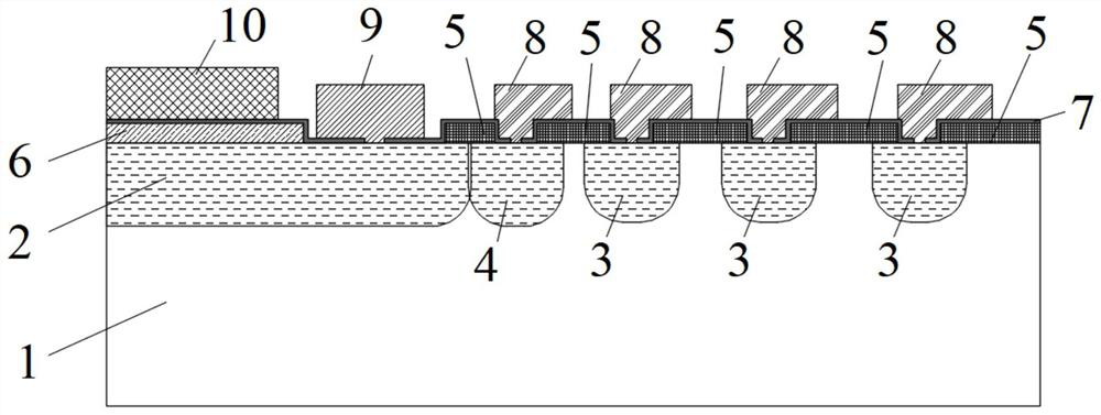
[0075] Such as figure 1 As shown, it is a cross-sectional schematic diagram of a junction terminal structure including a fusion resistor finally obtained by the manufacturing method provided by the embodiment of the present invention. The junction termination structure includes:
[0076] substrate layer 1,
[0077] A main junction ring 2, located in the surface layer of the substrate layer 1, and arranged in a racetrack shape;
[0078] N field-limiting rings 3 are located in the surface layer of the substrate layer 1, and are arranged in a racetrack shape on the periphery of the main junction ring, wherein N>1;
[0079] A fusion resistance ring 4 is located in the surface layer of the substrate layer 1, and is arranged in a racetrack between the main junction ring 2 and the field limiting ring 3; the main junction ring 2, the fusion resistance ring 4 and the field limiting ring 3 are arranged in sequence from the inside to the outside ;
[0080] The first-type field oxide r...
PUM
 Abstract
Description
Claims
Application Information
 - R&D
- Intellectual Property
- Life Sciences
- Materials
- Tech Scout
- Unparalleled Data Quality
- Higher Quality Content
- 60% Fewer Hallucinations
Browse by: Latest US Patents, China's latest patents, Technical Efficacy Thesaurus, Application Domain, Technology Topic, Popular Technical Reports.
© 2025 PatSnap. All rights reserved.Legal|Privacy policy|Modern Slavery Act Transparency Statement|Sitemap|About US| Contact US: help@patsnap.com


