Substrate detection device and method

A substrate inspection and detection device technology, applied in nonlinear optics, instruments, optics, etc., can solve problems such as TFT damage and damage

Active Publication Date: 2015-09-30
SHARP KK
View PDF6 Cites 9 Cited by
  • Summary
  • Abstract
  • Description
  • Claims
  • Application Information

AI Technical Summary

Problems solved by technology

For example, in a TFT liquid crystal display panel, when a wrong voltage is applied to the lead terminal due to misalignment, the TFT will be damaged depending on the time the voltage is applied
Therefore, due to the influence of deviations in the cutting position accuracy of the panel, when the panel is positioned according to the outline reference of the display panel and the detector is brought into contact, the TFT is frequently damaged due to the above-mentioned misalignment.

Method used


Image

  • Substrate detection device and method
  • Substrate detection device and method
  • Substrate detection device and method

Examples


Embodiment approach 1

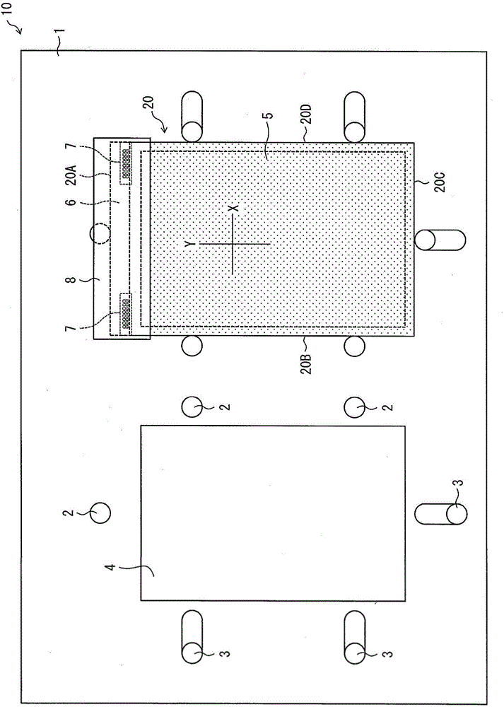
[0086] The substrate inspection and detection device of the present invention makes the probe contact the terminal of the inspection target substrate positioned based on the outer shape, and conducts electrical inspection (inspection of electrode disconnection, short circuit, etc.) by checking whether there is continuity between the terminal and the probe.

[0087] In this embodiment, as an example of such a substrate inspection probe device, a TFT panel substrate of a liquid crystal display panel is used as an inspection target substrate, and the electrical inspection performed is a lighting inspection of the liquid crystal display panel. In addition, the substrate to be inspected by the substrate inspection probe device of the present invention is not limited to the TFT panel substrate of the liquid crystal display panel, as long as it requires electrical inspection such as disconnection and short circuit of electrodes.

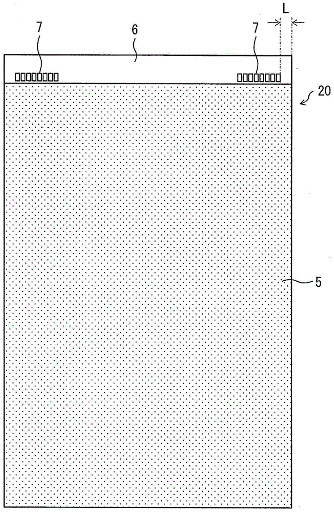
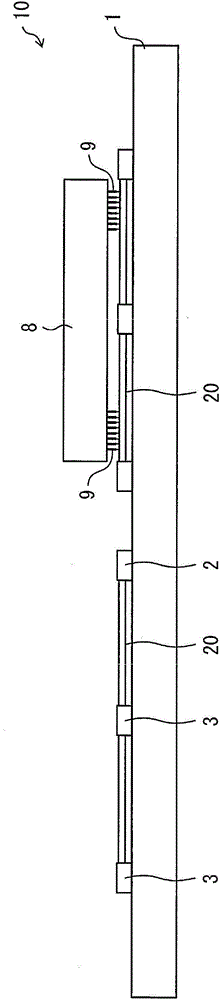
[0088] figure 1 It is a plan view showing a schemati...

Embodiment approach 2

[0128] based on Figure 8 to Figure 11 Another embodiment of the present invention will be described below. In addition, for convenience of description, members having the same functions as those described in the above-mentioned embodiments are denoted by the same reference numerals, and descriptions thereof are omitted.

[0129] Figure 8 It is a plan view showing a schematic configuration of an inspection module 30 to be inspected by the lighting inspection device 10A of the present embodiment. Figure 9 It is a plan view showing the schematic configuration of 10A of lighting inspection apparatuses of this embodiment. Figure 10 It is a side view which shows the schematic structure of 10 A of lighting inspection apparatuses of this embodiment. Figure 11 It is an enlarged plan view showing the configuration of an FPC (flexible printed circuit board) 22 for external driving in the inspection module 30 .

[0130] Such as Figure 8 As shown, the inspection module 30 includ...

Embodiment approach 3

[0153] based on Figure 12 and Figure 13 Still another embodiment of the present invention will be described below. In addition, for convenience of description, members having the same functions as those described in the above-mentioned embodiments are denoted by the same reference numerals, and descriptions thereof are omitted.

[0154] The lighting inspection device of the present embodiment is different from the first embodiment described above in that the detection portion is a detection FPC 32 including an FPC (flexible printed circuit board). Figure 12 The structure of the detection FPC 32 in the lighting inspection device of this embodiment is shown, Figure 12 (a) is a top view, Figure 12 (b) is a side view. in addition, Figure 13 It is a plan view schematically showing the state where the probe FPC 32 is in contact with the inspection terminal portion 7 in the lighting inspection device according to the present embodiment.

[0155] Such as Figure 12 and ...


PUM


Abstract

A substrate detection device and method are provided; when readjusting relative positions between a terminal and a detector, a CCD camera and a promotion mechanism need not to be aimed at; the substrate detection device comprises detector groups (a, c) matched with intervals of terminals forming a detection terminal portion; the detector groups are staggered in directions for arranging the terminals; the device is provided with a resistance measure portion (12) used for detecting a resistance value R between two terminals of the detection terminal portion (7); a switch (11) is arranged corresponding to each terminal.

Description

technical field [0001] The invention relates to a substrate inspection detection device and a substrate inspection method. Background technique [0002] In recent years, display panels have been installed in small and medium-sized digital products such as mobile phones, smartphones, and tablet computers. Such a display panel is manufactured by the following method. First, each of the CF panel substrate and the TFT panel substrate is produced on a so-called mother glass. Then, after laminating the CF panel substrate and the TFT panel substrate with a sealing material or the like, the CF panel substrate side is cut with a cutting wheel. Then, the mother glass is reversed, and the TFT panel substrate side is cut with a plurality of cutting wheels. Through such dicing, the bonded pair of substrates is cut into predetermined dimensions to manufacture a display panel. [0003] The cutting accuracy of the display panel may have a cutting deviation of ±0.1mm relative to the set ...

Claims


Application Information

Patent Timeline
Patent Type & Authority Applications(China)
IPC IPC(8): G02F1/13
CPCG02F1/1309
Inventor 相良智行
Owner SHARP KK
Why Eureka
Try Eureka