
A low-power inverter, low-power goa circuit and liquid crystal display panel

A technology of inverter and low power consumption, which is applied in the field of liquid crystal display to achieve the effect of shortening recovery time, increasing ESD protection ability, and avoiding short-circuit power consumption

Active Publication Date: 2018-05-29
WUHAN CHINA STAR OPTOELECTRONICS TECH CO LTD
View PDF11 Cites 0 Cited by
  • Summary
  • Abstract
  • Description
  • Claims
  • Application Information

AI Technical Summary

Problems solved by technology

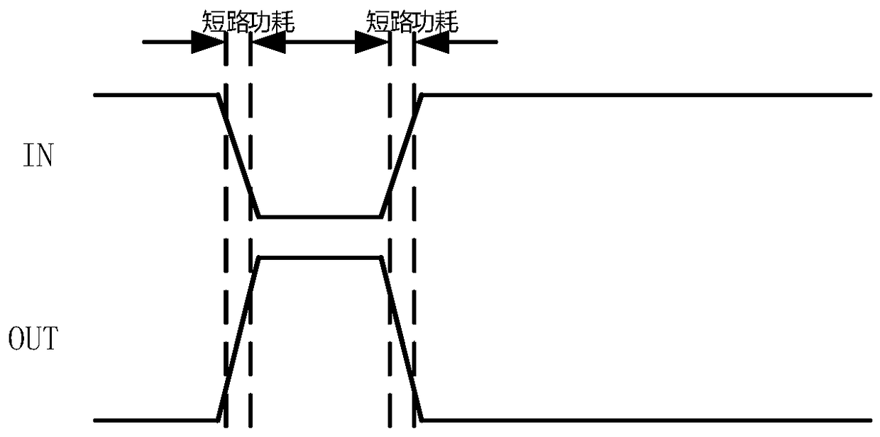
During the switching process of the inverter in the general CMOS circuit, the N-type transistor and the P-type transistor in the inverter will be turned on, resulting in a gap between the reference voltage input terminal of the P-type transistor and the reference input terminal of the N-type transistor. There is a short-circuit current in the short term, resulting in short-circuit power dissipation

Method used


Image

  • A low-power inverter, low-power goa circuit and liquid crystal display panel
  • A low-power inverter, low-power goa circuit and liquid crystal display panel
  • A low-power inverter, low-power goa circuit and liquid crystal display panel

Examples


Embodiment Construction

[0031] The implementation of the present invention will be described in detail below in conjunction with the accompanying drawings and examples, so as to fully understand and implement the process of how to apply technical means to solve technical problems and achieve technical effects in the present invention. It should be noted that, as long as there is no conflict, each embodiment and each feature in each embodiment of the present invention can be combined with each other, and the formed technical solutions are all within the protection scope of the present invention.

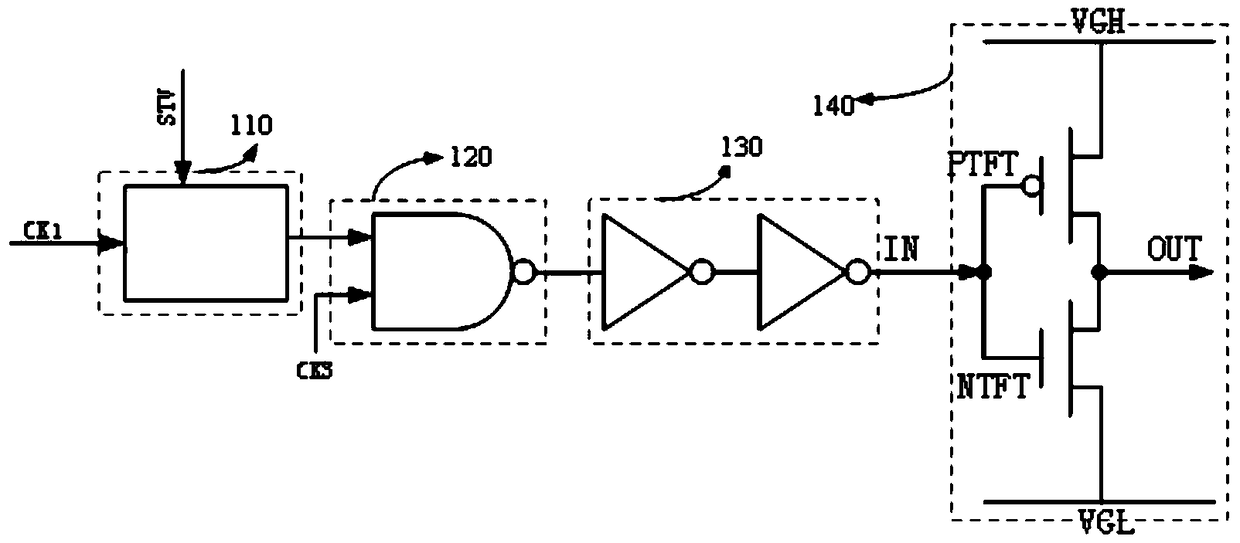
[0032] Such as figure 1 Shown is a schematic diagram of a CMOS GOA circuit structure commonly used in an existing general LTPS (low-temperature polysilicon, low-temperature polysilicon) process. Such as figure 1 As shown, the GOA circuit includes a latch 110 , a NAND signal processor 120 , a two-stage buffer 130 before output, and an inverter 140 . Among them, the latch 110 is used for latching the stage t...


PUM


Abstract

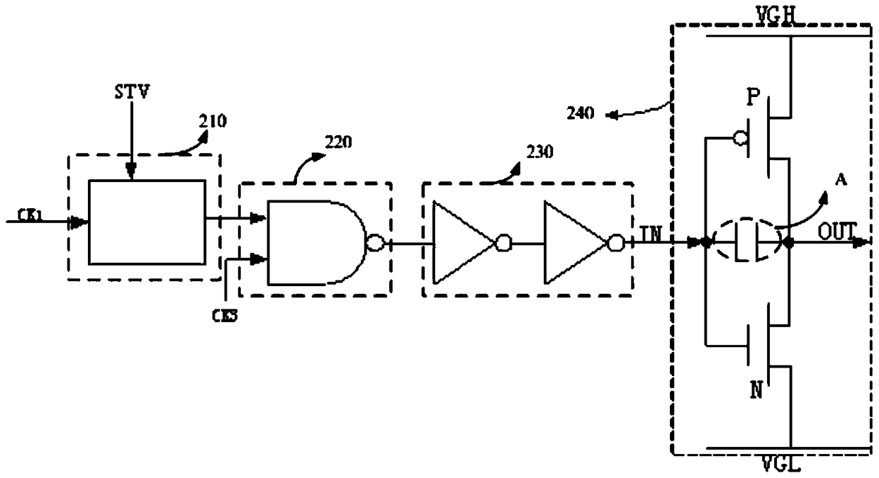
The invention discloses a low-power inverter, a low-power GOA circuit and a liquid crystal display panel. The low-power inverter includes: an inverter, which is composed of a P-type transistor and an N-type transistor in series, Wherein, a voltage coupling element is arranged between the input end and the output end of the inverter, so that when the voltage at the input end jumps, the voltage at the output end has a larger jump than the voltage at the input end. The invention can avoid the short-circuit power consumption of the inverter, shorten the recovery time of the inverter switch, improve the response speed of the circuit, and increase the ESD protection ability of the whole circuit.

Description

technical field [0001] The invention relates to the technical field of liquid crystal display, in particular to a low-power inverter, a low-power GOA circuit and a liquid crystal display panel. Background technique [0002] GOA (Gate Driver On Array, Gate Driver On Array) is a technology that utilizes the existing thin film transistor liquid crystal display array process to fabricate the gate line row scanning drive signal circuit on the array substrate to realize the gate line progressive scan drive method. [0003] In general low-temperature polysilicon technology LTPS process, a CMOS GOA circuit structure is commonly used, and the inverter at the end outputs a gate drive signal. During the switching process of the inverter in the general CMOS circuit, the N-type transistor and the P-type transistor in the inverter will be turned on, resulting in a gap between the reference voltage input terminal of the P-type transistor and the reference input terminal of the N-type trans...

Claims


Application Information

Patent Timeline
Patent Type & Authority Patents(China)
IPC IPC(8): G09G3/36
Inventor 赵莽易士娟
Owner WUHAN CHINA STAR OPTOELECTRONICS TECH CO LTD
Learn More