A one-bit full adder based on finfet mixed logic

A hybrid logic and full adder technology, applied in the direction of logic circuits with logic functions, etc., can solve the problems of increased circuit power consumption and delay, large power consumption and power consumption delay product, and increased key jump nodes.

Active Publication Date: 2018-08-14
NINGBO UNIV
View PDF3 Cites 0 Cited by
  • Summary
  • Abstract
  • Description
  • Claims
  • Application Information

AI Technical Summary

Problems solved by technology

However, the existing one-bit full adder based on CPL logic with the same gate of FinFET has the following problem: the one-bit full adder generates sum signal S and carry signal C by inversion O , it needs to be equipped with a FinFET tube that forms an inverter function, which will inevitably increase the key jump node, resulting in an increase in circuit power consumption and delay, and the power consumption and power consumption delay product are large

Method used


Image

  • A one-bit full adder based on finfet mixed logic
  • A one-bit full adder based on finfet mixed logic
  • A one-bit full adder based on finfet mixed logic

Examples


Embodiment 1

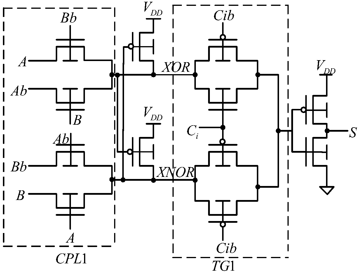
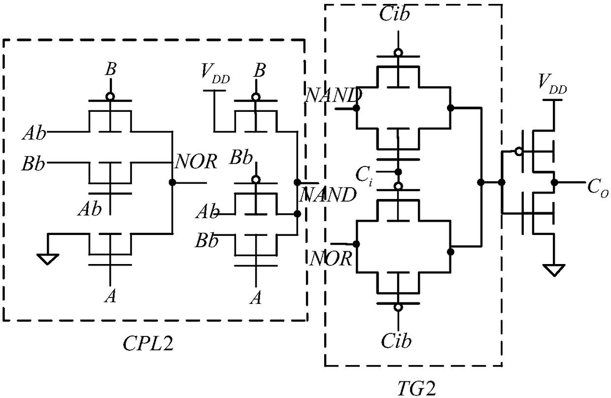
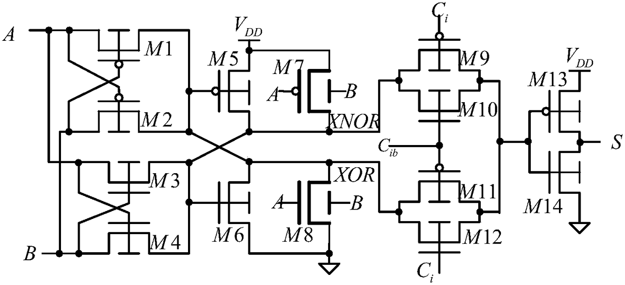
[0015] Embodiment one: if image 3 and Figure 4As shown, a one-bit full adder based on FinFET hybrid logic includes a summation output circuit and a carry output circuit. The summation output circuit includes a first FinFET tube M1, a second FinFET tube M2, a third FinFET tube M3, and a first FinFET tube M3. The fourth FinFET tube M4, the fifth FinFET tube M5, the sixth FinFET tube M6, the seventh FinFET tube M7, the eighth FinFET tube M8, the ninth FinFET tube M9, the tenth FinFET tube M10, the eleventh FinFET tube M11, the tenth The second FinFET tube M12, the thirteenth FinFET tube M13 and the fourteenth FinFET tube M14, the first FinFET tube M1, the second FinFET tube M2, the fifth FinFET tube M5, the seventh FinFET tube M7, the ninth FinFET tube M9, the The eleventh FinFET tube M11 and the thirteenth FinFET tube M13 are P-type FinFET tubes, the third FinFET tube M3, the fourth FinFET tube M4, the sixth FinFET tube M6, the eighth FinFET tube M8, the tenth FinFET tube M10...

Embodiment 2

[0016] Embodiment two: if image 3 and Figure 4As shown, a one-bit full adder based on FinFET hybrid logic includes a summation output circuit and a carry output circuit. The summation output circuit includes a first FinFET tube M1, a second FinFET tube M2, a third FinFET tube M3, and a first FinFET tube M3. The fourth FinFET tube M4, the fifth FinFET tube M5, the sixth FinFET tube M6, the seventh FinFET tube M7, the eighth FinFET tube M8, the ninth FinFET tube M9, the tenth FinFET tube M10, the eleventh FinFET tube M11, the tenth The second FinFET tube M12, the thirteenth FinFET tube M13 and the fourteenth FinFET tube M14, the first FinFET tube M1, the second FinFET tube M2, the fifth FinFET tube M5, the seventh FinFET tube M7, the ninth FinFET tube M9, the The eleventh FinFET tube M11 and the thirteenth FinFET tube M13 are P-type FinFET tubes, the third FinFET tube M3, the fourth FinFET tube M4, the sixth FinFET tube M6, the eighth FinFET tube M8, the tenth FinFET tube M10...


PUM


Abstract

The invention discloses a one-bit full adder based on Fin FET mixed logic. The one-bit full adder comprises a summing output circuit and a carry output circuit. The summing output circuit comprises first to fourteenth Fin FETs. The carry output circuit comprises fifteenth to twenty fourth Fin FETs. The one-bit full adder is low in power consumption and power consumption time delay product.

Description

technical field [0001] The invention relates to a one-bit full adder, in particular to a one-bit full adder based on FinFET hybrid logic. Background technique [0002] As a basic unit of an electronic system, a full adder can not only complete addition, but also participate in operations such as subtraction, multiplication, and division, and is widely used in large-scale integrated circuit design. The full adder is an important unit of a digital signal processor, a microprocessor, and a single-chip microcomputer system with relatively high performance requirements. The performance of the full adder has a particularly important impact on the performance of the entire system. One-bit full adder is widely used in the carry critical path of multi-bit adder, and is one of the important factors affecting multi-bit adder. FinFET tube (Fin Field-Effect Transistor, Fin Field-Effect Transistor) is a complementary metal oxide semiconductor (CMOS) transistor, which has the advantages o...

Claims


Application Information

Patent Timeline
Patent Type & Authority Patents(China)
IPC IPC(8): H03K19/20
CPCH03K19/20
Inventor 胡建平许仲池
Owner NINGBO UNIV
Why Eureka
Try Eureka