n-CdSxSe1-x film/graphene schottky junction solar cell
A technology of n-cdsxse1-x and solar cells, which is applied in the field of solar cells, can solve the problems of high cost of Schottky solar cells, and achieve the effects of low cost, simple preparation method, and high power generation efficiency
- Summary
- Abstract
- Description
- Claims
- Application Information
AI Technical Summary
Problems solved by technology
Method used
Image
Examples
Embodiment 2
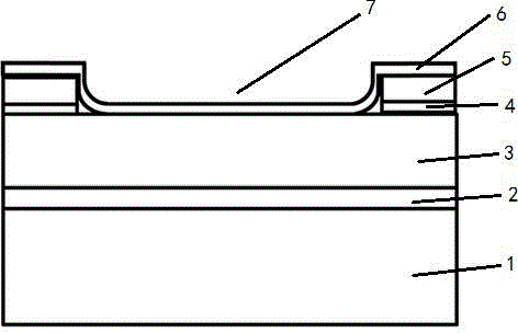
[0016] In Embodiment 2, a stainless steel sheet is used as the substrate 1, and the Mo back electrode 2 is deposited on the substrate 1 by electron beam evaporation process. Deposit a layer of Cd film on the back electrode 2 by evaporation process, and then anneal in Se, S atmosphere to form CdS 0.6 Se 0.4 Absorbing layer semiconductor thin film 3. CdS by sputtering x Se 1-x Depositing patterned Al on the film successively 2 o 3 Insulating layer 4 and gate line Au front electrode 5, and make it have through hole 7. Then the graphene film 6 is tiled on the above-mentioned grid line electrode 5, and through the through hole 7 and the CdS 0.6 Se 0.4 semiconductor thin film 3 contacts, and then in HNO 3 Treating for 2 minutes under the atmosphere to realize modification and modification of graphene, finally forming the Schottky junction thin-film solar cell device involved in the present invention.
PUM
 Abstract
Description
Claims
Application Information
