

Printed circuit board and network wire laying system
A technology for printed circuit boards and wires, which is applied in printed circuit parts, structural connections of printed circuits, printed circuits connected with non-printed electrical components, etc., which can solve the problem of poor torsional performance and low space utilization of multilayer PCBs and other issues, to achieve good mechanical properties, improve heat dissipation, and prevent easy falling off
- Summary
- Abstract
- Description
- Claims
- Application Information
AI Technical Summary
Problems solved by technology
Method used
Image

Examples
Embodiment 1
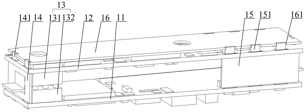
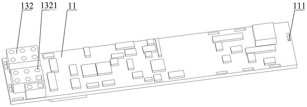
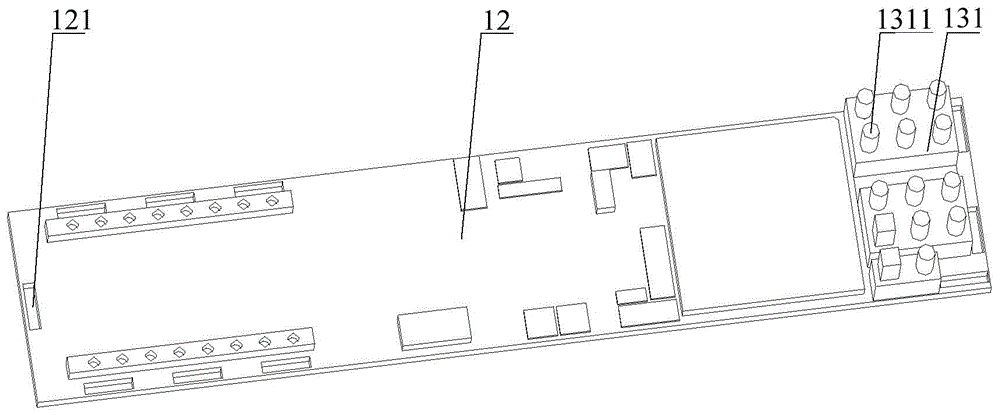
[0041] Please refer to the attached Figure 1-4 , figure 1 The structure of the printed circuit board provided by Embodiment 1 of the present invention is shown.
[0042] figure 1The printed circuit board shown includes a first PCB board 11 , a second PCB board 12 and a first connector. The first connecting piece is used for connecting the first PCB board 11 and the second PCB board 12 . The first connecting member is supported between the first PCB board 11 and the second PCB board 12 , so that a gap is formed between the first PCB board 11 and the second PCB board 12 . The gap is used to make the surfaces on both sides of the first PCB board 11 and the second PCB board 12 be the first installation surface for installing electronic components. That is, the opposite or opposite surfaces of the first PCB board 11 and the second PCB board 12 (ie, the inner and outer surfaces of the first PCB board 11 ) are used for mounting electronic components. In the same way, the two su...
Embodiment 2
[0056] Please refer to the attached Figure 5 , Figure 5 The structure of the printed circuit board provided by Embodiment 2 of the present invention is shown.
[0057] Figure 5 The printed circuit board shown includes a first PCB board 21 , a second PCB board 22 , a third PCB board 27 , a first connector and a second connector. The third PCB board 27 is located between the first PCB board 21 and the second PCB board 22 , and both surfaces of the third PCB board 27 are second installation surfaces for installing electronic components. The first connecting piece is used for connecting the first PCB board 21 and the second PCB board 22 . The first connecting member is supported between the first PCB board 21 and the second PCB board 22 , so that a gap is formed between the first PCB board 21 and the second PCB board 22 . The gap is used to make both surfaces of the first PCB board 21 and the second PCB board 22 be the first installation surface for installing electronic co...
Embodiment 3
[0073] Please refer to the attached Figure 6 , Figure 6 The wiring structure of the network wiring system provided by Embodiment 3 of the present invention is shown.
[0074] Figure 6 The network cabling system shown includes a first optical fiber, a first electrical wire, a second optical fiber, a second electrical wire, a printed circuit board and an optical splitter 38 .
[0075]Wherein: the printed circuit board is used to connect the first optical fiber and the second optical fiber, the first electric wire and the second electric wire (including electrical connection and optical signal connection), and the printed circuit board includes a first PCB board 31, a second PCB board 32 and first connector. The first connecting piece is used for connecting the first PCB board 31 and the second PCB board 32 . The first connecting member is supported between the first PCB board 31 and the second PCB board 32 , so that a gap is formed between the first PCB board 31 and the s...
PUM
 Abstract
Description
Claims
Application Information