
Preparation method for graphene touch screen

A graphene and touch screen technology, applied in the field of graphene touch screen preparation, can solve problems such as easy damage, inability to remove silver flakes, short circuit, surface dirt, easy scratches, etc., and achieve the effect of avoiding the increase of square resistance

Active Publication Date: 2015-10-07
CHONGQING GRAPHENE TECH +1
View PDF5 Cites 2 Cited by
  • Summary
  • Abstract
  • Description
  • Claims
  • Application Information

AI Technical Summary

Problems solved by technology

[0002] CVD polycrystalline graphene has poor adhesion to the substrate, and it is easy to scratch and damage in the pre-shrinking, silk printing, photolithography, cleaning and transfer production processes of conductive film touch screens. Normal cleaning (high-pressure water, ultrasonic, cleaning agent) solves the problem; cleaning will cause square resistance to increase or even a large area of ​​open circuit. Without cleaning, it is impossible to remove the short circuit of silver chips and surface dirt after photolithography. The yield rate is low, so it cannot be mass-produced. Produce

Method used


Image

  • Preparation method for graphene touch screen

Examples


Embodiment Construction

[0025] The principles and features of the present invention are described below in conjunction with the accompanying drawings, and the examples given are only used to explain the present invention, and are not intended to limit the scope of the present invention.

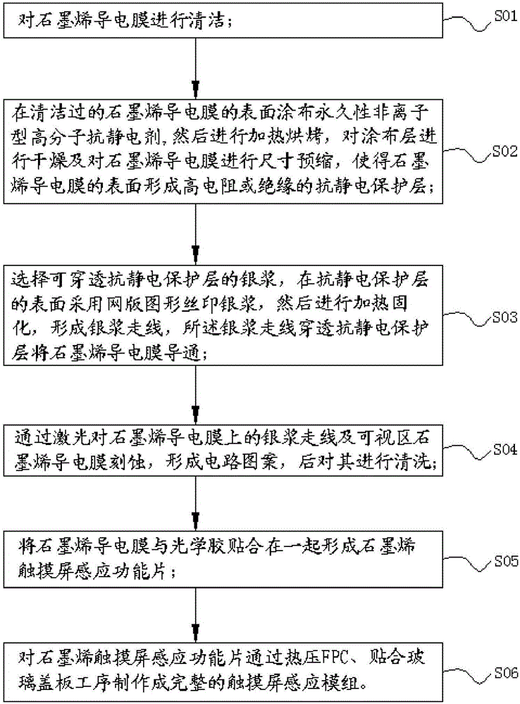
[0026] Such as figure 1 Shown, the present invention comprises the following steps:

[0027] S01, cleaning the graphene conductive film;

[0028] S02, coating a permanent non-ionic macromolecule antistatic agent on the surface of the cleaned graphene conductive film, then heating and baking, drying the coating layer and preshrinking the graphene conductive film, Form a high-resistance or insulating antistatic protective layer on the surface of the vinyl conductive film;

[0029] S03, select the silver paste that can penetrate the antistatic protective layer, use screen printing silver paste on the surface of the antistatic protective layer, and then heat and cure to form silver paste wiring, and the silver paste w...


PUM

PropertyMeasurementUnit
Particle sizeaaaaaaaaaa

Abstract

The present invention relates to a preparation method for a graphene touch screen. The method comprises: washing a graphene conductive film; coating a permanent non-ionic macromolecular anti-static agent on the surface of the graphene conductive film and heating and baking the coated conductive film to form a high-resistance or insulated anti-static protective layer; selecting silver paste capable of penetrating through the anti-static protective layer, printing the silver paste on the surface of the anti-static protective layer by a silkscreen, and heating and curing the silver paste to form a silver paste track, wherein the silver paste track penetrates through the anti-static protective layer to conduct the graphene conductive film; carrying out laser etching to form a circuit pattern; fitting the graphene conductive film to an optical adhesive; and producing a touch screen inductive module by steps of thermally pressing an FPC and fitting a glass cover plate. By means of the preparation method provided by the present invention, the high-resistance and even insulated anti-static protective layer is produced on the surface of the graphene conductive film, the silver paste capable of penetrating through the anti-static protective layer can penetrate through a conductive network formed by the anti-static protective layer to conduct graphene at the bottom, and normal use of the conductive film in the touch screen product and the preparation process is not influenced when the surface of the graphene is approximately insulated.

Description

technical field [0001] The invention relates to the technical field of graphene equipment, in particular to a method for preparing a graphene touch screen. Background technique [0002] CVD polycrystalline graphene has poor adhesion to the substrate, and it is easy to scratch and damage in the pre-shrinking, silk printing, photolithography, cleaning and transfer production processes of conductive film touch screens. Normal cleaning (high-pressure water, ultrasonic, cleaning agent) solves the problem; cleaning will cause square resistance to increase or even a large area of ​​open circuit. Without cleaning, it is impossible to remove the short circuit of silver chips and surface dirt after photolithography. The yield rate is low, so it cannot be mass-produced. Produce. Contents of the invention [0003] The technical problem to be solved by the present invention is to provide a method for preparing a graphene touch screen that is easy to clean and suitable for industrial m...

Claims


Application Information

Patent Timeline
IPC IPC(8): G06F3/041
Inventor 弋天宝余崇圣潘洪亮盖川史浩飞
Owner CHONGQING GRAPHENE TECH
Learn More