Long-distance LED lamp light modulation circuit through controllable rectification
A technology of LED lamps and dimming circuits, which is applied in the layout of electric lamp circuits, light sources, electric light sources, etc., can solve the problems of troublesome management, high cost, and large number of remote controllers.
- Summary
- Abstract
- Description
- Claims
- Application Information
AI Technical Summary
Problems solved by technology
Method used
Image

Examples
Embodiment Construction
[0041] The present invention will be described in further detail below with reference to the accompanying drawings and examples, but the embodiments of the present invention are not limited thereto.
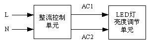
[0042] Realize the system structural block diagram of the present invention as figure 1 As shown, it consists of a rectifier control unit and an LED light brightness adjustment unit. The rectification control unit receives single-phase 220V AC power from phase line input terminal L and neutral line input terminal N, and outputs controllable rectification voltage from the first controllable rectification output terminal AC1 and the second controllable rectification output terminal AC2. The brightness adjustment unit of the LED lamp receives a controllable rectification voltage from the first controllable rectification input terminal AC1 and the second controllable rectification input terminal AC2 to control the brightness of the LED lamp.
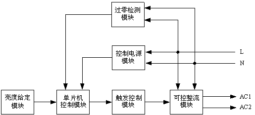
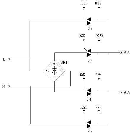
[0043] The structure of the rectifier c...
PUM
 Abstract
Description
Claims
Application Information
 - Generate Ideas
- Intellectual Property
- Life Sciences
- Materials
- Tech Scout
- Unparalleled Data Quality
- Higher Quality Content
- 60% Fewer Hallucinations
Browse by: Latest US Patents, China's latest patents, Technical Efficacy Thesaurus, Application Domain, Technology Topic, Popular Technical Reports.
© 2025 PatSnap. All rights reserved.Legal|Privacy policy|Modern Slavery Act Transparency Statement|Sitemap|About US| Contact US: help@patsnap.com