
Novel nanometer enhanced anti-sticking semiconductive non-woven fabric and processing technology thereof

A processing technology and semi-conductive technology, which is applied in the field of new nano-reinforced anti-adhesive semi-conductive non-woven fabric and its processing technology, can solve the problems of non-waterproof, surface bonding, melting, and small pulling force, so as to reduce production costs, Excellent electrical conductivity and high tensile strength

Inactive Publication Date: 2015-11-04
YANG ZHOU TENGFEI ELECTRIC CABLE & APPLIANCE MATERIALS CO LTD
View PDF0 Cites 0 Cited by
  • Summary
  • Abstract
  • Description
  • Claims
  • Application Information

AI Technical Summary

Problems solved by technology

[0002] Although the semi-conductive non-woven fabrics on the market have nanometer functions, their surface resistance and volume resistance are also very low, but the surface will bond and melt under instantaneous high temperature, without waterproof and anti-penetration functions of cable materials, and its pulling force is small. Not suitable for large cross-section and high-speed wrapping requirements

Method used

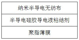
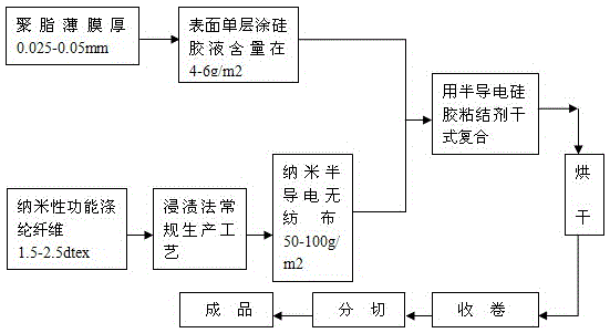
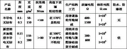

Image

  • Novel nanometer enhanced anti-sticking semiconductive non-woven fabric and processing technology thereof
  • Novel nanometer enhanced anti-sticking semiconductive non-woven fabric and processing technology thereof
  • Novel nanometer enhanced anti-sticking semiconductive non-woven fabric and processing technology thereof

Examples


Embodiment 1

[0023] The present invention carries out according to the following steps:

[0024] 1) First, weave nano-functional polyester fibers into nano-semiconductive non-woven fabrics, and the weight of the nano-semiconductive non-woven fabrics is;

[0025] 2) Coat the upper surface of the polyester film with anti-adhesive semi-conductive silica gel;

[0026] 3) Then, the nano-semiconductive non-woven fabric is compounded with a semi-conductive silicone adhesive and a polyester film by a compound machine, and then cut.

[0027] The thickness of the nano-functional polyester fiber is 2dtex, and the weight of the nano-semiconductive non-woven fabric is 80 g / m 2 .

[0028] The thickness of the polyester film is 0.04mm.

[0029] The amount of anti-adhesive semi-conductive silicone in the step 2) is 5g / m 2 .

[0030] In the step 3), the coating amount of the semi-conductive silicone adhesive is 8g / m 2 .

[0031] The composition ratio of the anti-adhesive semi-conductive silica gel i...

Embodiment 2

[0034] The present invention carries out according to the following steps:

[0035] 1) First, weave nano-functional polyester fibers into nano-semiconductive non-woven fabrics, and the weight of the nano-semiconductive non-woven fabrics is;

[0036] 2) Coat the upper surface of the polyester film with anti-adhesive semi-conductive silica gel;

[0037] 3) Then, the nano-semiconductive non-woven fabric is compounded with a semi-conductive silicone adhesive and a polyester film by a compound machine, and then cut.

[0038] The thickness of the nano-functional polyester fiber is 1.5dtex, and the weight of the nano-semiconductive non-woven fabric is 50 g / m 2 .

[0039] The thickness of the polyester film is 0.025mm.

[0040] The amount of anti-adhesive semi-conductive silicone in the step 2) is 4 g / m 2 .

[0041] In the step 3), the coating amount of the semi-conductive silicone adhesive is 10g / m 2 .

[0042] The composition ratio of the anti-adhesive semi-conductive silica ...

Embodiment 3

[0045] Follow the steps below:

[0046] 1) First, weave nano-functional polyester fibers into nano-semiconductive non-woven fabrics, and the weight of the nano-semiconductive non-woven fabrics is;

[0047] 2) Coat the upper surface of the polyester film with anti-adhesive semi-conductive silica gel;

[0048] 3) Then the nano-semiconductive non-woven fabric is compounded with a semi-conductive silicone adhesive with a compound machine, and cut into pieces.

[0049] The thickness of the nano-functional polyester fiber is 2.5dtex, and the weight of the nano-semiconductive non-woven fabric is 100 g / m 2 .

[0050] The thickness of the polyester film is 0.05mm.

[0051] The amount of anti-adhesive semi-conductive silicone in the step 2) is 6 g / m 2 .

[0052] In the step 3), the coating amount of the semi-conductive silicone adhesive is 8g / m 2 .

[0053] The composition ratio of the anti-adhesive semi-conductive silica gel is: 33% of silica gel, 55% of ethyl ester, 12% of cond...


PUM

PropertyMeasurementUnit
thicknessaaaaaaaaaa
Basis weightaaaaaaaaaa
thicknessaaaaaaaaaa

Abstract

The invention relates to novel nanometer enhanced anti-sticking semiconductive non-woven fabric and a processing technology thereof. The novel nanometer enhanced anti-sticking semiconductive non-woven fabric includes the following steps that firstly, nanometer functional polyester fibers are woven into the nanometer semiconductive non-woven fabric, and the gram weight of the semiconductive non-woven fabric is 50-100 g / m<2>; secondly, the upper surface of a polyester film is coated with sticking-preventing semiconductive silica gel; thirdly, the nanometer semiconductive non-woven fabric is compounded with the polyester film through a semiconductive silica gel bonding agent by a compound machine, and the novel nanometer enhanced anti-sticking semiconductive non-woven fabric is obtained through splitting. By means of the novel nanometer enhanced anti-sticking semiconductive non-woven fabric, the performance of a semiconductive electric material in a high-voltage cable can be optimized and improved, and the novel nanometer enhanced anti-sticking semiconductive non-woven fabric has the features of being semiconductive, capable of resisting water, capable of preventing sticking at a high temperature and the like; the production cost is reduced, cable recycling and classifying in the future are convenient due to the fact that interior adherence does not exist and products conform to the environmental-friendliness requirements of the European Union.

Description

technical field [0001] The invention relates to a novel nano-reinforced anti-adhesive semi-conductive non-woven fabric and its processing technology, which are mainly used in high-voltage mining cables and medium-voltage cables with large cross-sections. Background technique [0002] Although the semi-conductive non-woven fabrics on the market have nanometer properties, their surface resistance and volume resistance are also very low, but the surface will bond and melt under instantaneous high temperature, without waterproof and anti-penetration functions of cable materials, and its pulling force is small. It is not applicable to the requirements of large cross-section and high-speed wrapping. Contents of the invention [0003] In view of the above defects, the present invention aims to provide a new type of nano-reinforced anti-adhesive semi-conductor with excellent electrical conductivity, high tensile strength, waterproof, anti-penetration, anti-acid and alkali, anti-ra...

Claims


Application Information

Patent Timeline
Patent Type & Authority Applications(China)
IPC IPC(8): D04H1/435D04H1/58H01B5/14
Inventor 张云周敏玉徐鹭鹭王华平杨正龙张玉梅王彪陈仕艳陈晓浪
Owner YANG ZHOU TENGFEI ELECTRIC CABLE & APPLIANCE MATERIALS CO LTD
Learn More