Conductive module, preparation method thereof, substrate and display device

A technology of conductive components and substrates, which is applied in semiconductor/solid-state device manufacturing, electrical components, semiconductor devices, etc., can solve the problems of reduced effective display area, increased process times, and alignment difficulties, so as to reduce reflectivity and avoid process times , Improve the effect of display contrast

Active Publication Date: 2015-11-11
BOE TECH GRP CO LTD
View PDF4 Cites 15 Cited by
  • Summary
  • Abstract
  • Description
  • Claims
  • Application Information

AI Technical Summary

Problems solved by technology

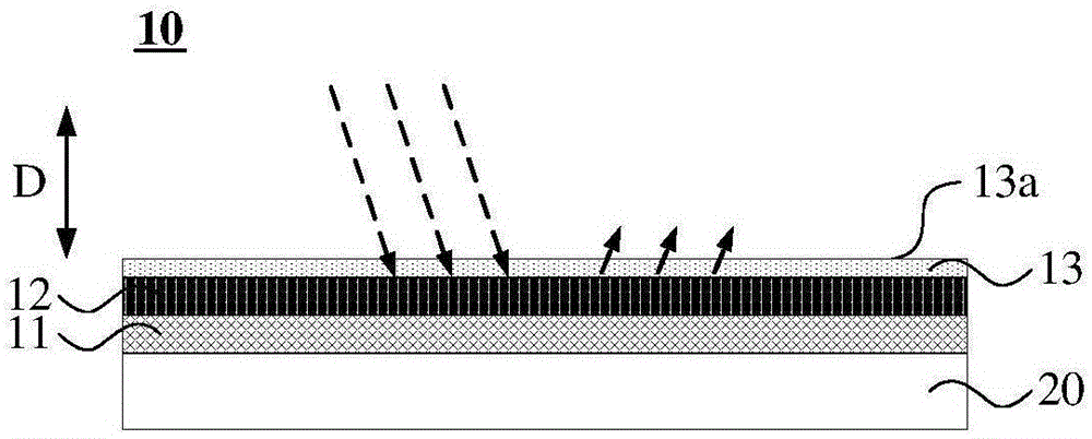
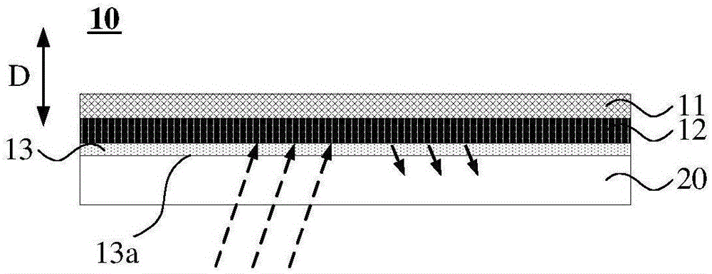
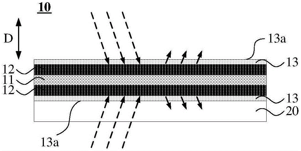
[0006] In view of this, in order to solve the problems of the prior art, embodiments of the present invention provide a conductive component and its preparation method, a substrate, and a display device. The conductive component has a good anti-reflection effect on incident light. When the conductive component When the component is applied to the conductive patterns in the display device, such as metal traces and other electrode structures, there is no need to additionally set up a black matrix, which avoids many problems such as increased number of processes, difficult alignment, and reduced effective display area due to the black matrix.

Method used


Image

  • Conductive module, preparation method thereof, substrate and display device
  • Conductive module, preparation method thereof, substrate and display device
  • Conductive module, preparation method thereof, substrate and display device

Examples


Embodiment Construction

[0040] The following will clearly and completely describe the technical solutions in the embodiments of the present invention with reference to the accompanying drawings in the embodiments of the present invention. Obviously, the described embodiments are only some, not all, embodiments of the present invention. Based on the embodiments of the present invention, all other embodiments obtained by persons of ordinary skill in the art without making creative efforts belong to the protection scope of the present invention.

[0041] It should be noted that, unless otherwise defined, all terms (including technical and scientific terms) used in the embodiments of the present invention have the same meaning as commonly understood by those of ordinary skill in the art to which the present invention belongs. It should also be understood that terms such as those defined in common dictionaries should be interpreted as having meanings consistent with their meanings in the context of the rel...


PUM

PropertyMeasurementUnit
refractive indexaaaaaaaaaa

Abstract

The embodiment of the invention provides a conductive module, a preparation method thereof, a substrate and a display device, relating to the technical field of display. When the conductive module is applied to a metal wiring equivalent-electrode structure in the display device, a black matrix cannot be needed to additionally arranged, and the problems of increase on process flows due to the arrangement of the black matrix, difficulty in alignment, effective reduction on display area and the like are avoided. The conductive module comprises a metal layer, a light absorption layer and an antireflection layer, wherein the light absorption layer and the antireflection layer are sequentially arranged on at least one side surface of the metal layer, the refractive index of the light absorption layer is greater than that of the antireflection layer, and the antireflection layer is far away from a first surface of the light absorption layer and close to a light incident direction. The preparation method is used for preparation of the conductive module, the substrate containing the conductive module and the display device containing the conductive module.

Description

technical field [0001] The invention relates to the field of display technology, in particular to a conductive component, a preparation method thereof, a substrate, and a display device. Background technique [0002] Structures such as gate lines, data lines, and common electrode lines in the array substrate are usually made of metal materials with low resistivity. Since metal materials have a certain reflection effect on light, it is also necessary to additionally arrange a black matrix for blocking light on the array substrate or the color filter substrate that is boxed with the array substrate. [0003] The material of the black matrix can be composed of carbon black particles or metal materials with low reflectivity such as molybdenum (Mo) and chromium (Cr). The reflectance of these two materials to light is quite different. The reflectivity of carbon black particles to light is less than 5%, while the reflectivity of metal materials such as Mo and Cr to light is greate...

Claims


Application Information

Patent Timeline
Patent Type & Authority Applications(China)
IPC IPC(8): H01L21/28H01L27/32
CPCH01L21/28H10K59/12G02F1/133502G02F2201/08G02F2201/38G02F1/134381G02F1/134372G02F1/136222H10K59/38H10K59/131H10K50/865H10K50/86H01L21/2855H01L21/7685H01L21/76877H01L23/528H01L23/53223H01L27/124H01L27/1259G02F1/13362G02F1/136286H01L23/53238H01L23/53266
Inventor 张锋
Owner BOE TECH GRP CO LTD
Why Eureka
Try Eureka