Semiconductor chip integrated element

A technology of integrated components and semiconductors, which is applied in the direction of semiconductor devices, semiconductor/solid-state device parts, electrical components, etc., and can solve problems such as solder overflow, abnormal packaging structures, and low product qualification rate

Pending Publication Date: 2015-11-11
SHENZHEN BENCENT ELECTRONICS CO LTD
View PDF4 Cites 2 Cited by
  • Summary
  • Abstract
  • Description
  • Claims
  • Application Information

AI Technical Summary

Problems solved by technology

[0004] The embodiment of the present application provides a semiconductor chip integrated component, which solves the problems of dislocation connection, serious solder overflow phenomenon and low product qualification rate caused by many abnormal packaging structures when the existing semiconductor chip integrated component packages the semiconductor chip

Method used


Image

  • Semiconductor chip integrated element
  • Semiconductor chip integrated element
  • Semiconductor chip integrated element

Examples


Embodiment Construction

[0033] The technical solutions in the embodiments of the present application will be clearly and completely described below in conjunction with the drawings in the embodiments of the present application. Apparently, the described embodiments are only some of the embodiments of the present application, not all of them. Based on the embodiments in this application, all other embodiments obtained by persons of ordinary skill in the art without making creative efforts belong to the scope of protection of this application.

[0034] In the following, specific examples will be used to describe in detail respectively.

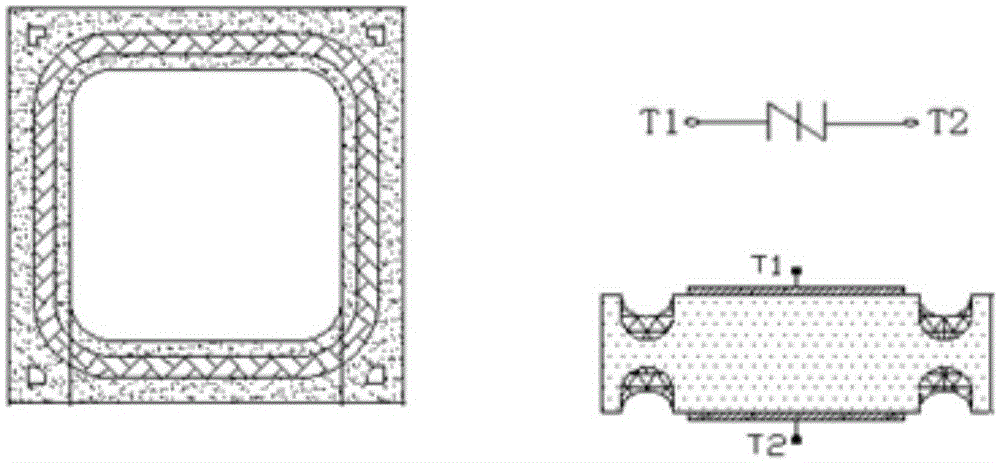
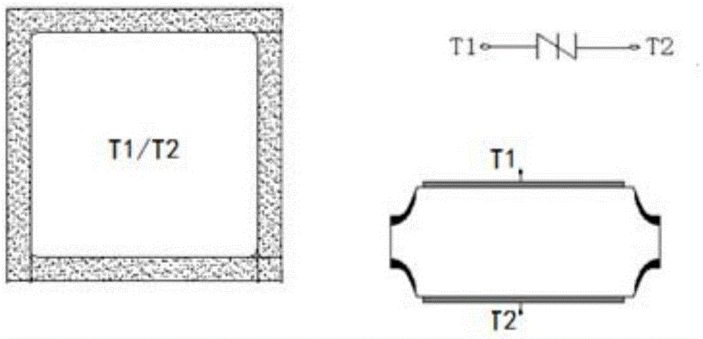
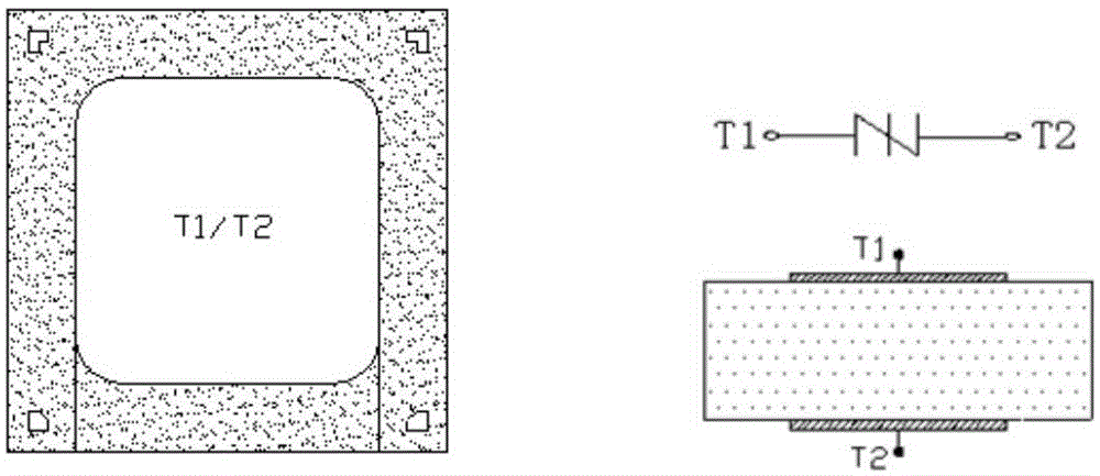
[0035] On the one hand, the semiconductor chip integrated component provided by the embodiment of the present application includes, from top to bottom, a first lead structure, a second lead structure, and N third lead structures stacked between the first lead structure and the second lead structure, N is an integer greater than or equal to 0; the first lead structure, ...


PUM


Abstract

The embodiment of the invention discloses a semiconductor chip integrated element. The semiconductor chip integrated element includes a first lead structure, a second lead structure and N third lead structures which are stacked between the first lead structure and the second lead structure; one semiconductor chip is connected between chip trays of every two adjacent lead structures, so that a plurality of semiconductor chips can be packaged in an integrated manner so as to form the semiconductor chip integrated element; the lower surface of the chip tray of the first lead structure is provided with a first boss in fit connection with the electrode of the semiconductor chip; the upper surface of the chip tray of the second lead structure is provided with a second boss in fit connection with the electrode of the semiconductor chip; and the upper surface and the lower surface of the chip tray of each third lead structure are respectively provided with a third boss in fit connection with the electrode of the semiconductor chip. With the above technical schemes of the invention adopted, packaging of semiconductor chips of various kinds of structures can be realized, and the problems of mal-posed connection and solder overflow in semiconductor chip packaging can be solved.

Description

technical field [0001] The present application relates to the field of semiconductor chip integrated components, in particular to a semiconductor chip integrated component. Background technique [0002] Thyristor surge suppressor (Thyristor Surge Suppressor, TSS), also known as solid discharge tube or semiconductor discharge tube, is a cutting-edge product of lightning protection devices in the communication field. When the external lightning induced voltage rises to its breakdown voltage, the semiconductor discharge tube The curve action of an avalanche triode can flow a large surge current or pulse current, and its breakdown voltage range is the overvoltage protection range. [0003] In this technical field, the chips that constitute the semiconductor discharge tube are divided into three structures according to their physical characteristics, which are Figure 1a shows the inner trench chip, Figure 1b shows the outer trench chip and Figure 1c A planar chip is shown, w...

Claims


Application Information

Patent Timeline
IPC IPC(8): H01L23/498H01L23/49H01L23/488
CPCH01L2924/181H01L23/488H01L23/49H01L23/498H01L2924/00014H01L24/37H01L2224/37599H01L2924/00012H01L2224/37099
Inventor 苟引刚王久黎永阳高桂丽
Owner SHENZHEN BENCENT ELECTRONICS CO LTD
Why Eureka
Try Eureka