Manufacturing method for array substrate and array substrate

一种阵列基板、制作方法的技术,应用在液晶显示领域,能够解决降低生产效率、制作流程繁杂、增加阵列基板与彩膜基板制作流程等问题,达到降低生产成本、提高生产效率的效果

Inactive Publication Date: 2015-11-18
TCL CHINA STAR OPTOELECTRONICS TECH CO LTD +1
View PDF5 Cites 6 Cited by
  • Summary
  • Abstract
  • Description
  • Claims
  • Application Information

AI Technical Summary

Problems solved by technology

However, in the prior art, when manufacturing the color filter substrate, four pixels of R, G, B, and W need to be prepared separately before forming a flat layer, and the manufacturing process is relatively complicated; in addition, because the array substrate and the color filter During the manufacturing process of the substrate, it is necessary to form a flat layer on the surface of each color resist of the color filter substrate and the surface of the control electrode of the array substrate, so two flat layer processes are required, which increases the cost of the array substrate and the color filter substrate. production process, thereby reducing production efficiency

Method used


Image

  • Manufacturing method for array substrate and array substrate
  • Manufacturing method for array substrate and array substrate
  • Manufacturing method for array substrate and array substrate

Examples


Embodiment Construction

[0038] The present invention will be further described below in conjunction with accompanying drawing.

[0039] The particulars presented here are exemplary and used for illustrative discussion of embodiments of the invention only, and are presented to provide what is believed to be the most useful and understandable description of the principles and conceptual aspects of the invention. Regarding this point, there is no attempt to introduce the structural details of the present invention beyond the level required for a basic understanding of the present invention. Those skilled in the art can clearly understand how to implement the present invention in practice through the description and accompanying drawings. Several forms.

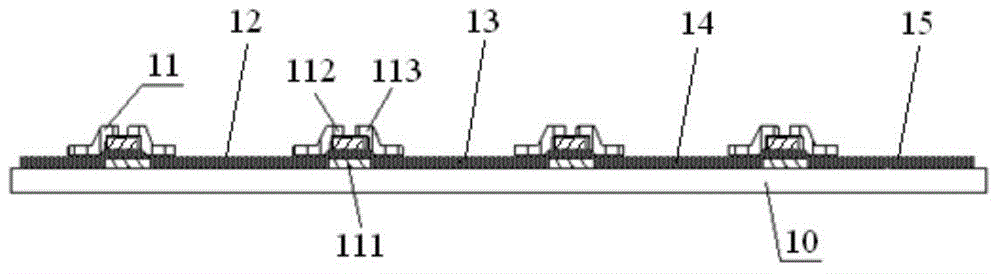
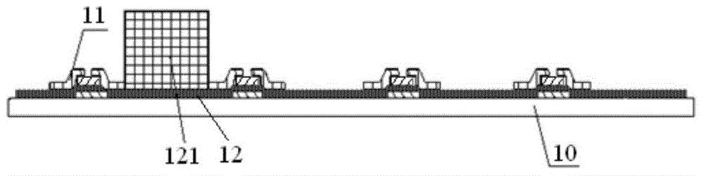
[0040] figure 1 A method for fabricating an array substrate according to the present invention is shown, and here a-SiFFS (amorphous silicon fringe field switch) technology is taken as an example for specific illustration. Specifically include the fol...


PUM


Abstract

The invention discloses a manufacturing method for an array substrate and the array substrate. The method includes the steps that a plurality of control electrodes are formed on the substrate so that a first color resistance area, a second color resistance area, a third color resistance area and a fourth color resistance area are formed between adjacent control electrodes respectively; a first color resistor is formed on the first color resistance area, a second color resistor is formed on the second color resistance area and a third color resistor is formed on the third color resistance area in sequence; the substrate where the control electrodes, the first color resistor, the second color resistor and the third color resistor are formed, and the fourth color resistance area are internally coated with transparent color resistors to form a flat layer. The manufacturing method further improves production efficiency of the array substrate.

Description

technical field [0001] The invention belongs to the technical field of liquid crystal display, and in particular relates to a manufacturing method of an array substrate and an array substrate. Background technique [0002] RGBW technology adds W pixels (transparent pixels) on the basis of RGB (three-color pixel technology). The white light emitted by the backlight increases the output rate of the white light, that is, increases the brightness of the liquid crystal display panel. [0003] The way of RGBW technology in the prior art is to form four pixels of R, G, B, and W on the color filter substrate, and then apply a transparent resin material on the color filter substrate as a flat layer. On the one hand, the flat layer It can be used as a protective layer and a flat layer for each pixel. On the other hand, its transparent material can allow the light passing through the W pixel to pass through the flat layer. However, in the prior art, when manufacturing the color filte...

Claims


Application Information

Patent Timeline
Patent Type & Authority Applications(China)
IPC IPC(8): G02F1/1343G02F1/1362
CPCG02F1/134309G02F1/136209G02F1/136227G02F1/1362G02F1/133357G02F1/136231G02F1/136222G02F1/0063G02F1/133516G02F1/133621G02F1/1343
Inventor 明星
Owner TCL CHINA STAR OPTOELECTRONICS TECH CO LTD
Why Eureka
Try Eureka