Wafer dewaxing device and dewaxing method

A wafer and dewaxing technology, applied in the manufacture of electrical components, electric solid-state devices, semiconductor/solid-state devices, etc., can solve the problems of energy waste, waste of manpower, etc., to reduce labor intensity, facilitate operation, and facilitate installation and disassembly.

Inactive Publication Date: 2015-11-18
TIANJIN XINTUO ELECTRONICS SCI & TECH
View PDF0 Cites 1 Cited by
  • Summary
  • Abstract
  • Description
  • Claims
  • Application Information

AI Technical Summary

Problems solved by technology

Existing dewaxing equipment uses belts or manual transportation when transferring wafers between different processes, which has the problem of energy waste, and at the same time, it is a waste of manpower

Method used


Image

  • Wafer dewaxing device and dewaxing method

Examples


Embodiment 1

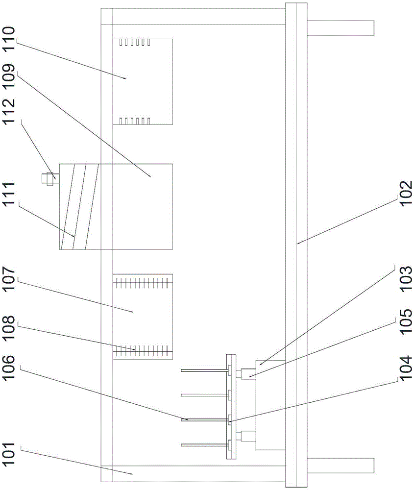
[0033] In order to collect wax conveniently, in this embodiment, preferably, a dust removal device is provided at the end of the exhaust port at the upper end of the high-temperature gasification box 107 .

[0034] Further preferably, the dust removal device includes a condensation plate 111 connected to the exhaust port and a dust removal exhaust port 112 arranged on the upper part of the condensation plate 111 . By adopting the condensation plate, after the wax is vaporized at high temperature, it gathers on the condensation plate, which is convenient for centralized treatment.

[0035] In order to facilitate fixing the installation bar, in this embodiment, preferably, the installation groove 104 is a T-shaped slot, and the lower end of the installation bar 106 is clamped in the installation groove 104 .

[0036] Further preferably, a resistance wire is arranged inside the installation strip 106 . By arranging the resistance wire, the mounting bar can be heated, so that the...

Embodiment 2

[0039] An integrated wafer dewaxing method, comprising the following steps:

[0040] S1: install the chip: install the chip on the mounting bar 106, and snap the mounting bar 106 into the mounting groove (104), so that the mounting bar 106 is fixed relative to the mounting groove 104;

[0041] S2: Push the fixed plate 103 to move along the guide rail 102. When the fixed plate 103 reaches the bottom of the electromagnetic heating box 107, start the hydraulic cylinder 105 to push the installation groove 104 and the installation bar 106 to move up as a whole until the wafer is completely placed in the electromagnetic heating box 107 Inside, carry out electromagnetic heating to remove wax;

[0042] S3: after step S2, place the wafer in the high-temperature vaporization box 107, and vaporize the remaining wax on the wafer at high temperature;

[0043] S4: The wafers after step S3 are placed in the hot air drying box 110, and then output after hot air drying treatment.


PUM


Abstract

The invention discloses an integrated wafer dewaxing device which comprises a frame and a guide rail arranged on the lower portion of the frame. A fixing plate capable of moving along the guide rail is arranged on the guide rail, a hydraulic cylinder is arranged on the fixing plate, installing grooves are arranged on the hydraulic cylinder, and a mounting bar for installing a wafer is arranged in the installing groove. An electromagnetic heating case body is arranged on the frame, and an electromagnetic heating coil is arranged in the electromagnetic heating case body and attached to the inside wall of the electromagnetic heating case body. A high temperature gasification case body is arranged on the frame, a high temperature hot gas nozzle is arranged on the sidewall of the high temperature gasification case body, and an air exhaust opening is arranged in the upper end of the high temperature gasification case body. The wafer dewaxing device is integrated, and continuous operation of multiple processes is realized. The dewaxing effect is improved, and energy can be effectively saved.

Description

technical field [0001] The invention relates to wafer dewaxing equipment and a dewaxing method. Background technique [0002] The method of dewaxing the wafer by heating usually requires multiple operations to achieve the desired effect. When the existing dewaxing equipment transfers the wafers between different processes, it adopts belt or manual transportation, which has the problem of wasting energy and wastes manpower at the same time. Contents of the invention [0003] The object of the present invention is to provide a wafer dewaxing equipment and dewaxing method, which can improve the problems existing in the prior art. By adopting the integrated equipment, the continuous operation of multiple processes can be realized, the dewaxing effect can be improved, and energy can be effectively saved at the same time. [0004] The present invention is realized through the following technical solutions: [0005] An integrated wafer dewaxing equipment, comprising a frame and...

Claims


Application Information

Patent Timeline
Patent Type & Authority Applications(China)
IPC IPC(8): H01L21/677H01L21/67H01L21/02
CPCH01L21/67126H01L21/02H01L21/67155H01L21/67703H01L2221/67
Inventor 张明
Owner TIANJIN XINTUO ELECTRONICS SCI & TECH
Why Eureka
Try Eureka